Do you have a question about the Silicon Laboratories C8051F32x and is the answer not in the manual?
Step-by-step guide to running the Blinky example project.
Instructions on accessing integrated help and documentation within Simplicity Studio.
Details on installing and configuring the legacy 8-bit IDE and Keil tools.
Configuration options for internal and external system clock sources on the target board.
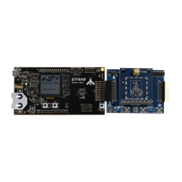
Description and function of the board's switches, LEDs, and potentiometer.
Pin definitions and functionality of the USB connector (J14).
Overview of the 32-pin expansion I/O connector (J1) and its pin assignments.
How to configure the target board for power via USB instead of an AC/DC adapter.
Details on the DEBUG connector (J4) for debugging and programming.
Description of the RS232 transceiver and UART0 connections via connector J5.
Pin descriptions for the analog I/O terminal block (J6).
Information on powering the target board using the USB Debug Adapter connector (J8).
| Core Architecture | 8051 |
|---|---|
| Flash Memory | 32 KB |
| GPIO Pins | 32 |
| ADC Channels | 8 |
| DAC | No |
| Communication Interfaces | UART, SPI, I2C |
| Operating Voltage | 2.7 V to 3.6 V |
| Temperature Range | -40 °C to +85 °C |
| Package | LQFP, QFN |
| ADC Resolution | 10-bit |