DRAFT D
TNM-M-E-0001 Page 22
3.4.2 DSP Clock Oscillator
The DSP is clocked by a 15.360MHz oscillator which consists of crystal X100 and an internal
DSP oscillator. Q100 forms a crystal switching circuit with C117 which when activated by a
command from the FPGA steers the oscillator away from potential interfering frequencies.
3.5 Memory
Memory consists of the internal DSP memory and an external 4MB non-volatile Flash Memory
U104. When power is off, program and data is retained in Flash Memory. At power-on, a boot
program downloads the DSP’s program from Flash Memory to its internal RAM for faster
program execution and access to data.
3.5.1 Multiplexer
U902 contains 2 separate 4-channel multiplexers providing a total of 8 independently controlled
analog switches. Under software control, the multiplexers produce tuning voltages from supplied
data for the receiver front end (TUNE 1 to 4), TX power setting (TX PWR SET), receiver AGC
(AGC-1), alert tone (A TONE) and FPGA ramp generator (ADC REF).
Buffer U802B is fed with a composite digital tuning signal (AUX CTL) from the DSP/FPGA
containing the data for AGC, A TONE, ADC REF and TX PWR SET settings. The level is
dependent on channel frequency and tuning and varies between 0.1 to 3.0V. This signal is
applied to one group of 4 analog switches in U902 via a common input connected to pin 13. The
second group of 4 switches is fed with the receiver front end tuning signal FE TUNE (to provide
outputs for TUNE 1 to 4) via the second common input at pin 3 as described in the receiver front
end section.
The 2 groups of analog switches are independently controlled by FPGA binary signals MUX A0
and A1 and enable line MUXEN to output the required tuning voltages as a series of pulses.
These pulses are converted to steady state voltages by integration capacitors C904 to 911 and
C921 to 925.
3.6 Power Supplies
3.6.1 Power On Function
The unregulated 13.8V DC input is routed directly to high current devices and is also switched
via FET Q350. The output from Q350 feeds three, low drop out series regulators and associated
switched and auxiliary supplies which along with a negative voltage generator provide all the
switched power requirements of the transceiver.
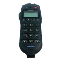
Q315/316/317 and U313 form a power on/off latch circuit which is activated by a pulse from the
control unit or microphone/handset via PWR ON or PWR OFF and controls the FET power
switch Q350. A PWR OFF operation requires the button to be held down for more than 2
seconds. This is then sensed by the FPGA via the PWR SENSE line which turns the radio off by
placing a positive pulse on the PWR OFF line thereby resetting U313B.