SiT-AN6722EB Manual Rev. 2.0
SiT6722EB Evaluation Board User Manual
2 I/O Descriptions
Table 1. SiT6722EB I/O
SMA connector (J1), a two-pin connector (P5) for DC power supply.
Pins polarities are identified on the silkscreen pattern near the connector
(see A1 and A2). Two-pin headers (P3, P4).
A two-pin header (P7) provides access to the pin 1 of the Super-TCXO in either
OE mode or VCTCXO mode. In OE mode, pin 1 can be left floating as there is an
internal pull-up resistor
Frequency control
via I
2
C
A five-pin header (P9) provides access to I
2
C (SDA, SCL)
Oscillator output can be accessed either using active probe or SMA connector.
The test points for active probe are placed closely to the oscillator output for
better signal integrity (see Figure A2). The output pin of the oscillator can also
be connected to the SMA connector (J2) through the R9 source termination
resistor.
describes in details the recommended measurement
A two-pin connector (P6) enables measuring the current consumption of the
device.
P1, P2, P3, P4 are reserved for SiTime internal use only.
3 EVB Usage Descriptions
3.1 EVB Configurations
SiT6722EB can be configured to support all three Super-TCXO configuration modes including TCXO with
output enable (OE), VCTCXO with analog voltage control and DCTCXO with I
2
C.
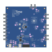
Figure A1 in Appendix A shows the complete electrical schematic of SiT6722EB. Components labeled
“DNP” are not assembled.
Oscillator output waveform can be measured with an active probe in all configurations. The value of the
load capacitor C5 can be adjusted to match the load conditions in the target application. This enables
the user to measure waveform characteristics under similar conditions as close to those on the target
board as possible.
Shipment Configuration
SiT6722 is shipped without components labeled “DNP” on the schematic (see in Appendix A). Figure A1