* The value of the load capacitor C3 and load resistor R11 can be adjusted to match the load conditions
in the target application. This enables the user to measure waveform characteristics under similar
conditions as close to those on the target board as possible.
** LVCMOS-to-sinewave filter components values will depend on the carrier frequency of the device.
Contact SiTime to get recommended nominals for filter components.
The test points for active probe are placed closely to the oscillator output for better signal integrity (see
Figure A2).
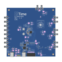
Figure A1 in Appendix A shows the complete electrical schematic of SiT6731EB. Components labeled
“DNP” are not assembled.
Shipment Configuration
SiT6731EB is shipped configured for buffered output allowing connecting it to the instrument input using
50 Ω coax cable. Details on the board assembly for shipment configuration can be found on the schematic
(see Figure A1 in Appendix A). C5, R13 and R14 values would depend on the signaling type selected for the
particular device configuration.
 Loading...