SiT6731EB Manual Rev. 3.0
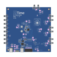
SiT6731EB Evaluation Board User Manual
2 I/O Descriptions
Table 1. SiT6731EB I/O
Four -pin connector (P1) for DC power supply and power sensing.
VDD is connected to Pin 1, GND – to Pin2 of P1.
VDD sense is connected to Pin 4, GND – to Pin3 of P1.
Two-pin connector (P2) provides access to the pin 1 of the OCXO in OE mode.
In OE mode, pin 1 can be left floating as there is an internal pull-up resistor.
Frequency
control via I
2
C
A three-pin header (P3) provides access to I
2
C (SDA, SCL) bus for DCOCXO
configuration.
Oscillator output can be accessed in several ways:
- Direct output through SMA connector
- Buffered output through SMA connector
- Oscilloscope probe at probing points
- Direct output through LVCMOS-to-sinewave filter and SMA
connector
Please refer to the Section 3.1 for the details.
P4, P5 is reserved for SiTime internal use only.
3 EVB Usage Descriptions
3.1 EVB Configurations
SiT6731EB comes designed to support OCXO and DCOCXO devices.
Oscillator output can be accessed in several ways listed in Table 1. Table 2 describes components
configuration to support all output configurations.