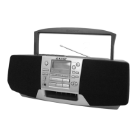
CFD-S350/S350L
23 23
CFD-S350/S350L
TUNER board
TC board
BATT-1 board
BATT-2 board
MAIN board
LCD board
POWER KEY board
CD KEY board
H/P board
POWER board
CD board
6-5. CIRCUIT BOARDS LOCATION• NOTE FOR PRINTED WIRING BOARDS AND SCHEMATIC DIAGRAMS
THIS NOTE IS COMMON FOR PRINTED WIRING
BOARDS AND SCHEMATIC DIAGRAMS.
(In addition to this, the necessary note is
printed in each block.)
for schematic diagram:
• All capacitors are in µF unless otherwise noted. (p: pF)
50 WV or less are not indicated except for electrolytics
and tantalums.
• All resistors are in Ω and
1
/
4
W or less unless otherwise
specified.
•
f
: internal component.
• C : panel designation.
• A : B+ Line.
• H : adjustment for repair.
•Voltage and waveforms are dc with respect to ground
under no-signal conditions.
– CD Board –
no mark : CD PLAY
– TUNER Board –
no mark : FM
(): AM (MW)
<>: LW
– Other Boards –
no mark : FM
(): PB
<>: REC
[]: CD PLAY
•Voltages are taken with a VOM (Input impedance 10 MΩ).
Voltage variations may be noted due to normal produc-
tion tolerances.
•Waveforms are taken with a oscilloscope.
Voltage variations may be noted due to normal produc-
tion tolerances.
• Circled numbers refer to waveforms.
• Signal path.
F : FM
f : AM (MW/LW)
E : PB
a : REC
J : CD PLAY
•Abbreviation
CND : Canadian model.
E92 : AC 120V area in E model.
AUS: Australian model.
KR : Korean model.
MX : Mexican model.
SP : Singapore model.
TH : Thai model.
TW : Taiwan model.
for printed wiring boards:
• X : parts extracted from the component side.
• Y : parts extracted from the conductor side.
• W : indicates side identified with part number.
•
f
: internal component.
• : Pattern from the side which enables seeing.
(The other layer’s patterns are not indicated.)
C
B
These are omitted.
E
Q
B
These are omitted.
C
Q
Q
E
BCE
Note: The components identified by mark 0 or dotted line
with mark 0 are critical for safety.
Replace only with part number specified.
Caution:
Pattern face side: Parts on the pattern face side seen from
(Conductor Side) the pattern face are indicated.
Parts face side: Parts on the parts face side seen from
(Component Side) the parts face are indicated.
• Waveforms
1.8Vp-p
1 IC2 w; (XOUT)
0.5V/div, 5
µ
sec/div
75kHz
— CD BOARD — (CD PLAY)
— TUNER BOARD —
— MAIN BOARD —
— TC BOARD —
0.85
±
0.2Vp-p
Approx. 100mVp-p
1
IC701 4 (RF)
500mV/div, 0.5
µ
sec/div
1.8V
Approx. 100mVp-p
1.8V
16.93MHz
3.2Vp-p
2
IC701 qd (FE)
100mV/div, 20
µ
sec/div
3
IC701 qg (TE)
100mV/div, 20
µ
sec/div
4
IC701 rk (XOUT)
1V/div, 0.05
µ
sec/div
19.5
µ
sec
4Vp-p
1
Q301 C (REC)
0.1V/div, 5
µ
sec/div
19.5
µ
sec
40Vp-p
2
T301, HRP301 (YEL)
10V/div, 5
µ
sec/div
1.5Vp-p
1.2Vp-p
4.19MHz32.768kHz
1
IC801 ua (XT2)
2V/div, 10
µ
sec/div
2
IC801 ug (X2)
2V/div, 10
µ
sec/div
(CFD-S350)
(CFD-S350L)
Ver. 1.1
 Loading...