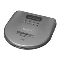
D-V8000
– 17 – – 18 –
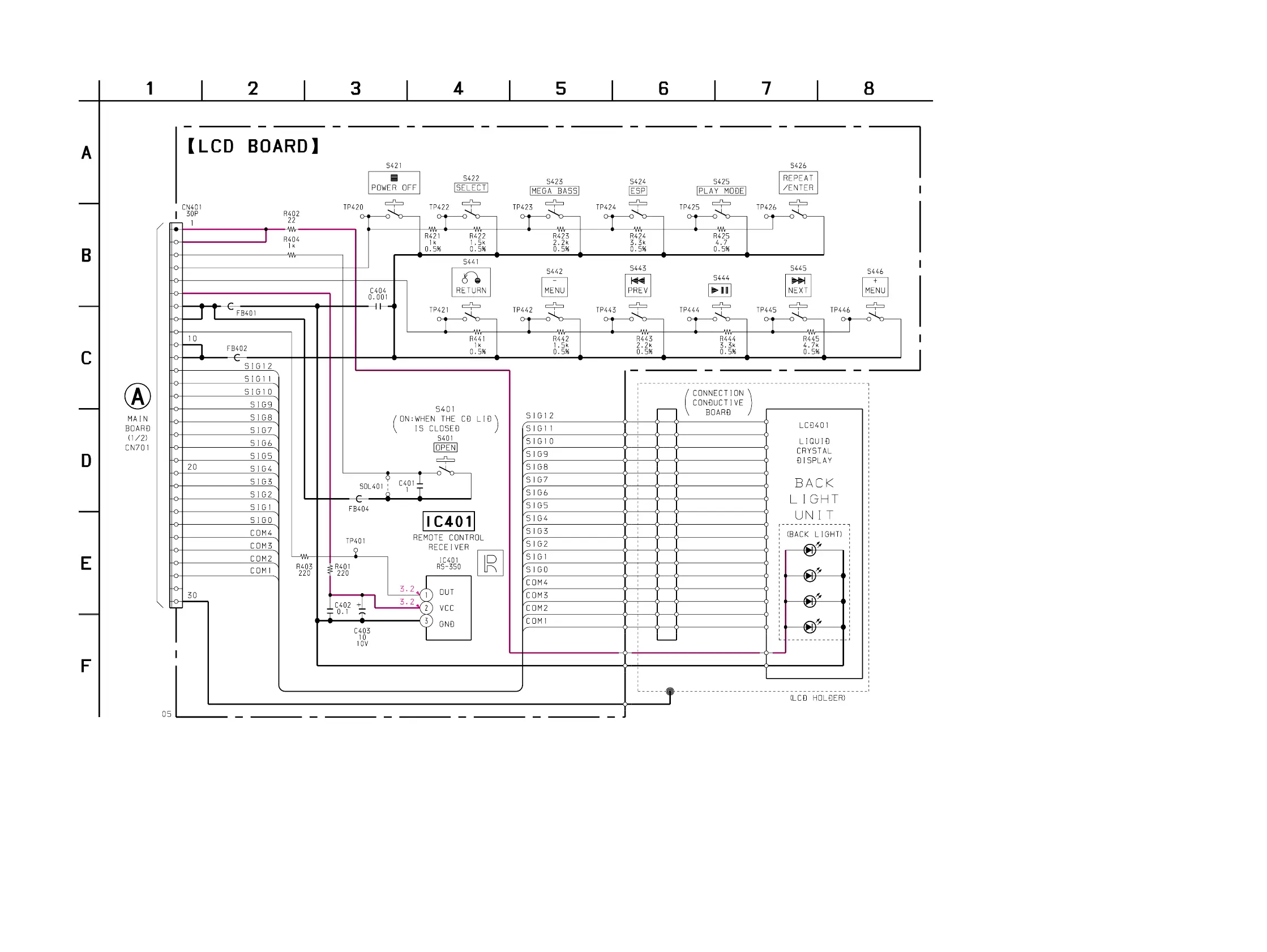
2-6. SCHEMATIC DIAGRAM – LCD BOARD –
Note on Schematic Diagram:
• All capacitors are in µF unless otherwise noted. pF: µµF
50 WV or less are not indicated except for electrolytics
and tantalums.
• All resistors are in Ω and
1
/
4
W or less unless otherwise
specified.
• % : indicates tolerance.
• C : panel designation.
• A : B+ Line.
• Power voltage is dc 6 V and fed with regulated dc power
supply from external power voltage jack.
• Voltages and waveforms are dc with respect to ground
under no-signal conditions.
no mark : VIDEO CD PLAY
• Voltages are taken with a VOM (Input impedance 10 MΩ).
Voltage variations may be noted due to normal produc-
tion tolerances.
(Page 11)


 To Next Page