DSX-A50BT
DSX-A50BT
1616
THIS NOTE IS COMMON FOR PRINTED WIRING BOARDS AND SCHEMATIC DIAGRAMS.
(In addition to this, the necessary note is printed in each block.)
For Printed Wiring Boards.
Note:
• X : Parts extracted from the component side.
• Y : Parts extracted from the conductor side.
•
f
: Internal component.
•
: Pattern from the side which enables seeing.
(The other layers’ patterns are not indicated.)
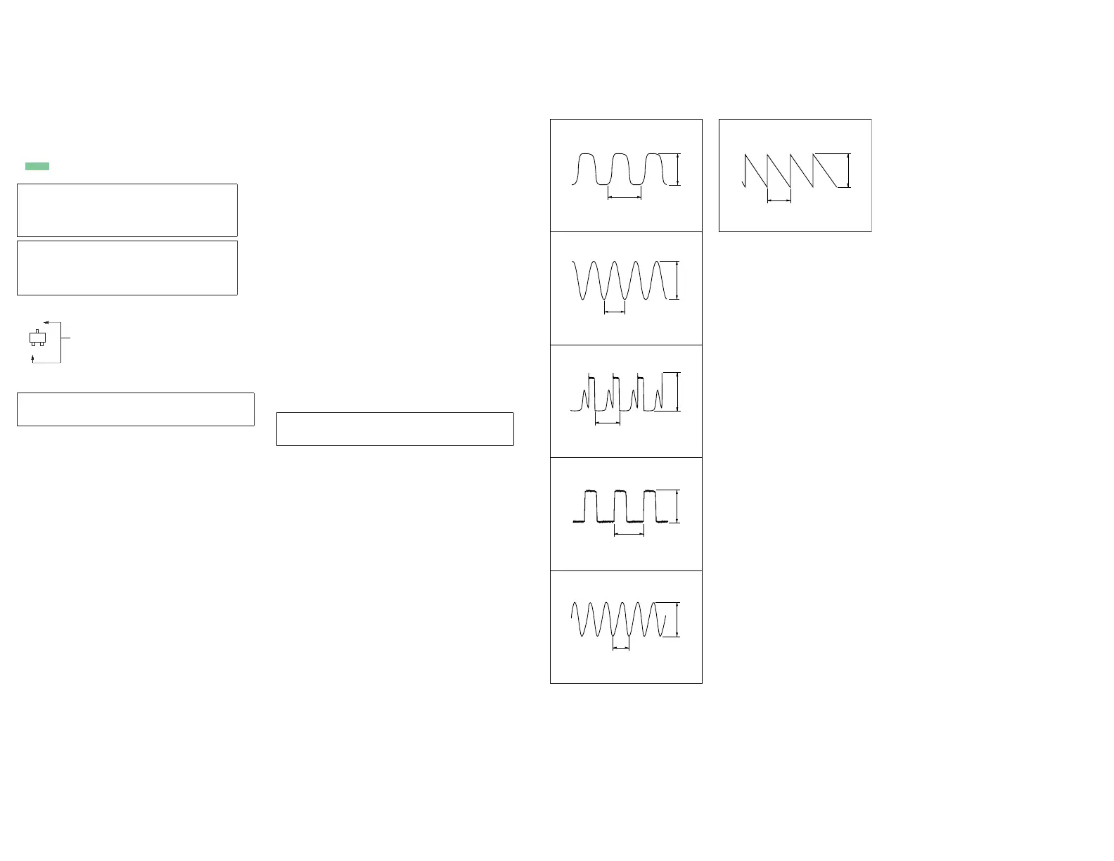
• Waveforms
– MAIN Board –
For Schematic Diagrams.
Note:
• All capacitors are in —F unless otherwise noted. (p: pF)
50 WV or less are not indicated except for electrolytics
and tantalums.
• All resistors are in : and
1
/4 W or less unless otherwise
specifi ed.
•
f
: internal component.
• C : panel designation.
• A : B+ Line.
• Power voltages is dc 14.4V and fed with regulated dc
power supply from ACC and BATT cords.
• Voltages and waveforms are dc with respect to ground
under no-signal (detuned) conditions.
no mark
: TUNER
• Voltages are taken with a VOM (Input impedance 10 M:).
Voltage variations may be noted due to normal production
tolerances.
• Waveforms are taken with a oscilloscope.
Voltage variations may be noted due to normal production
tolerances.
• Circled numbers refer to waveforms.
• Signal path.
F : AUDIO
f : TUNER
d : USB
E : AUX
a : Bluetooth
N : MIC
• Abbreviation
IND : Indian model
Caution:
Pattern face side:
(Conductor Side)
Parts face side:
(Component Side)
Parts on the pattern face side seen
from the pattern face are indicated.
Parts on the parts face side seen from
the parts face are indicated.
• Indication of transistor.
C
B
These are omitted.
E
Q
2
IC101 qa (OSCOUT)
1 V/DIV, 50 ns/DIV
126 ns
3.5 Vp-p
1
IC101 9 (XOUT)
1 V/DIV, 20 Ps/DIV
30.5 Ps
2.5 Vp-p
3
IC501 1 (BST), 2 (LX)
5 V/DIV, 1 Ps/DIV
2.4 Ps
18.2 Vp-p
4
IC501 8 (SYNC)
1 V/DIV, 1 Ps/DIV
2.4 Ps
3.3 Vp-p
5
IC201 ug (X12OUT)
1 V/DIV, 50 ns/DIV
83 ns
3.2 Vp-p
qa
IC901 rf (OSC)
1 V/DIV, 10 Ps/DIV
28.4 Ps
2.6 Vp-p
– KEY Board –
• Abbreviation
IND : Indian model
Note:
When the MAIN board in this unit is replaced, the destination
setting is necessary. Refer to “NOTE THE MAIN BOARD OR
SYSTEM CONTROLLER (IC101) REPLACING” (page 4).
Note:
When the MAIN board in this unit is replaced, the destination
setting is necessary. Refer to “NOTE THE MAIN BOARD OR
SYSTEM CONTROLLER (IC101) REPLACING” (page 4).
Caution:
Pattern face side:
(SIDE B)
Parts face side:
(SIDE A)
Parts on the pattern face side seen
from the pattern face are indicated.
Parts on the parts face side seen from
the parts face are indicated.
 Loading...