1818
ICD-U50/U60/U70
ICD-U50/U60/U70
• IC Block Diagrams
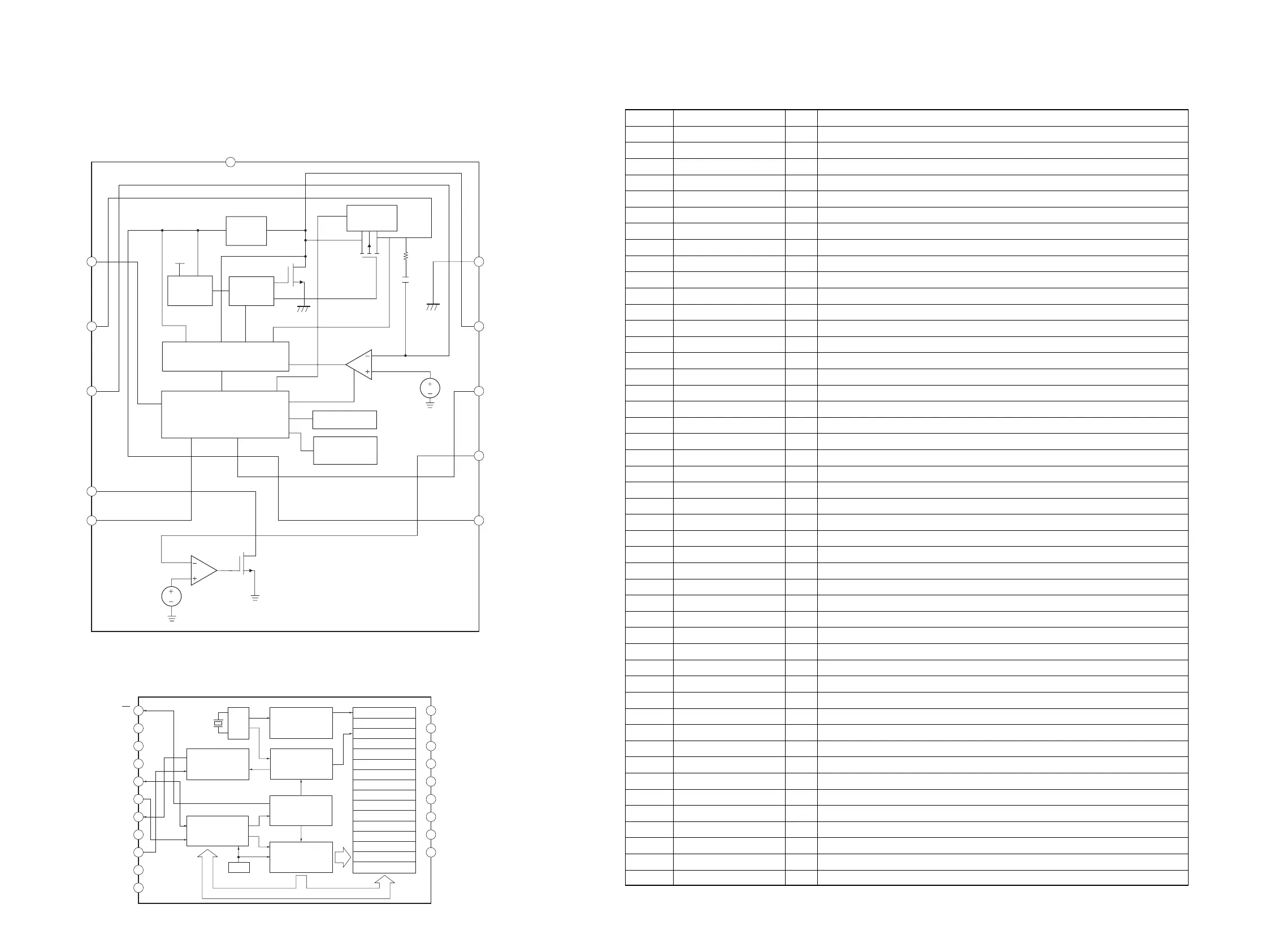
– MAIN Board –
IC501 TPS61020DRCR
IC703 RTC8564NB
EN
Anti-
Ringing
Backgate
Control
VOUT
Vmax
Control
Gate
Control
Regulator
Control Logic
Oscillaor
Temperature
Control
Vref=0.5V
Error
Amplifier
PGND
PGND
20pF
10kΩ
GND
Low Battery
Comparator
Vref=0.5V
GND
GND
1
2
VOUT
3
FB
4
LBO
5
GND
10
PGND
9
SW
8
PS
7
LBI
6
VBAT
10
1
2
3
4
5
6
7
8
9
20
19
18
17
16
15
14
13
12
10
OSC
32.768kkHz
CRYSTAL
POR
OUTPUT
CONTROL
Voltage Detector
Control 1
Control 2
Seconds
Minutes
Hours
Days
Weekdays
Month/Century
Years
Minutes Alarm
Hour Alarm
Day Alarm
Weekend Alarm
CLKOUT frequency
Timer Control
Timer 0F
DIVIDER
CONTROL
LOGIC
ADDRESS
REGISTER
I
2
C-BUS
INTERFACE
GND1
INT
GND2
NC1
SDA
SCL
CLKOUT
VDD
CLKOE
NC2
NC3
NC4
NC5
NC6
NC7
NC8
NC9
NC10
NC11
NC12
11
00
• IC Pin Function Description
MAIN BOARD IC701 DE53SN589AM8BLC (SYSTEM CONTROLLER)
Pin No. Pin Name I/O Description
1 SPOUTP O Speaker output
2BCLK O Not used (open)
3 TXMOD O Not used (open)
4 RSSI I Not used (connected to ground)
5 XIN I Clock input terminal (4.096MHz)
6 XOUT O Clock output terminal (4.096MHz)
7 VDD — DSP core power supply output terminal
8 VCCIN — DSP core power supply terminal
9 GND1 — Ground terminal for digital circuit
10 USBP I/O USB data signal (+)
11 USBM I/O USB data signal (–)
12 VCC1 — Power supply terminal for digital circuit
13 DCDCGND — LCD backlight LED drive ground
14 DCDCIN I LCD backlight LED drive power supply terminal
15 DCDCOUT O LCD backlight LED drive (Pull up)
16 RSTN I/O External reset signal input and output
17 BGPIO0 O Chip enable signal output for NAND Flash Memory pull-up terminal
18 BGPIO3 O Address latch enable signal output for NAND Flash Memory
19 BGPIO4 O Command latch enable signal output for NAND Flash Memory
20 BGPIO5 O Not used
21 BGPIO6 O Chip enable signal output for NAND Flash Memory (Not used)
22 EGPIO14 I Test mode start signal input (for factory use)
23 BGPIO1 O [PLAY] LED drive control signal output
24 BGPIO2 O [REC] LED drive control signal output
25 BGPIO11 I/O Not used (open)
26 BGPIO12 O Not used (open)
27 BGPIO13 O Headphones mute control signal output
28 BGPIO15 O Not used (open)
29 CGPIO3 I USB connection detect signal input
30 GND2 — Ground terminal for digital circuit
31 VCC2 — Power supply terminal for digital circuit
32 EGPIO12 O LCD controller chip select signal output
33 EGPIO13 O LCD controller serial clock signal output
34 EGPIO11 O LCD controller serial data signal output
35 BGPIO7 O LCD controller address signal output
36 BGPIO8 O External speaker mute control signal output (not used)
37 BGPIO9 O External speaker shutdown control signal output (not used)
38 BGPIO10 I NAND Flash Memory Ready/Busy signal input
39 DGPIO10 I/O NAND Flash Memory CS1/CS2 select signal input (not used)
40 DGPIO9 O USB connection detect signal input
41 DGPIO8 I RTC interrupt input
42 DGPIO7 I/O NAND Flash Memory data bus
43 DGPIO6 I/O NAND Flash Memory data bus
44 DGPIO5 I/O NAND Flash Memory data bus
45 DGPIO4 I/O NAND Flash Memory data bus
46 DGPIO3 I/O NAND Flash Memory data bus
47 DGPIO2 I/O NAND Flash Memory data bus
Ver. 1.1