19
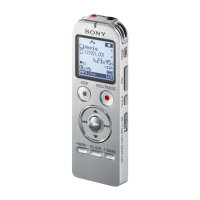
ICD-U50/U60/U70
48 DGPIO1 I/O NAND Flash Memory data bus
49 DGPIO0 I/O NAND Flash Memory data bus
50 GND3 — Ground terminal for digital circuit
51 VCC3 — Power supply terminal for digital circuit
52 DRDN O Read enable signal output for NAND Flash Memory
53 DWRN O Write protect signal output to NAND Flash Memory
54 AGPIO1 O Not used (open)
55 AGPIO3 O RTC clock output acknowledge output
56 AGPIO4 O MIC power control signal output
57 AGPIO5 O MIC sensitivity select signal output
58 AGPIO6 I
REC/PAUSE
key signal input
59 AGPIO7 I
NX
key signal input
60 AGPIO8 I
STOP
key signal input
61 AGPIO9 I
>
key signal input
62 EGPIO7 I
.
key signal input
63 EGPIO8 I
A-B
key signal input
64 EGPIO9 I
VOL+
key signal input
65 EGPIO10 I
VOL–
key signal input
66 EGPIO15 I
z , MENU
key signal input
67 GND4 — Ground terminal for digital circuit
68 VCC4 — Power supply terminal for digital circuit
69 TCK I JTAG clock signal input (Pull up)
70 TMS I JTAG mode select signal input (Pull down)
71 TDI I JTAG data input (Pull down)
72 TDO O JTAG data output (Pull up)
73 DGPIO15 I USB resume detection signal input
74 DGPIO14 I WAKE UP interrupt input
75 DGPIO13 I HOLD switch signal input
76 DGPIO12 I DPC switch signal input
77 DGPIO11 I Headphones detect signal input
78 AGPIO0 I Pull down
79 AGPIO2 I Pull down
80 AGPIO10 O I
2
C clock input for RTC control
81 AGPIO11 I/O I
2
C data input/output for RTC control
82 AGPIO12 O Test mode control UART data output (not used)
83 AGPIO13 I Test mode control UART data input (Pull down)
84 BGPIO14 O USB control signal output
85 GND5 — Ground terminal for digital circuit
86 DCIN3/PDN I Not used (connected to ground)
87 DCIN1/IBAT I Battery voltage detect and battery consumption detect signal input
88 VREF O Reference voltage output terminal for analog circuit
89 MIP I MIC signal input
90 MIN I Not used
91 DCIN2/MPWR I Not used
92 GNDA — Ground terminal for analog circuit
93 VCCA — Power suplly for analog circuit
94 LINO I Not used (connected to ground)
95 DCINO I Not used (connected to ground)
96 LOUT0 O Headphones [L] signal output
Pin No. Pin Name I/O Description