EasyManua.ls Logo

Sony MHC-D7 - Page 54

Sony MHC-D7
85 pages
Print Icon
To Next Page IconTo Next Page
To Previous Page IconTo Previous Page
Loading...
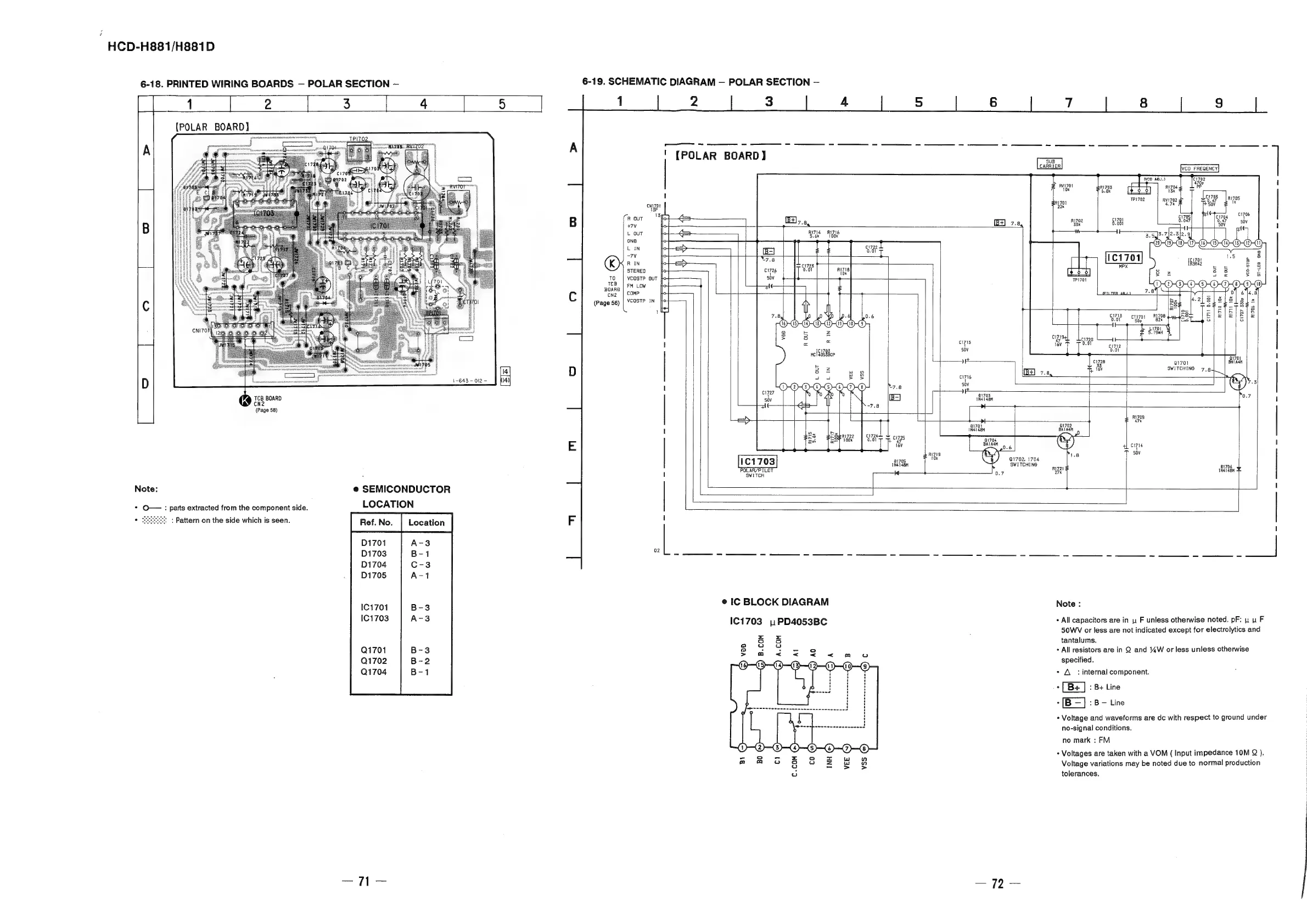
HCD-H881/H881D
6-18.
PRINTED
WIRING
BOARDS
—
POLAR
SECTION
—
6-19.
SCHEMATIC
DIAGRAM
—
POLAR
SECTION
—
D1705
1C1701
1C1703
Q1704
e
IC
BLOCK
DIAGRAM
1C1703
1.
PD4053BC
Note
:
+
All
capacitors
are
in
y
F
unless
otherwise
noted.
pF:
yu
F
50WV
or
less
are
not
indicated
except
for
electrolytics
and
°
5
5
tantalums.
pelbed
2
om
ee CS
+
All
resistors
are
in
Q
and
YW
or
less
unless
otherwise
Q1702
@
specified.
-
A:
internal
component.
.
:
B+
Line
.
:B-
Line
*
Voltage
and
waveforms
are
dc
with
respect
to
ground
under
no-signal
conditions.
no
mark
:
FM
+
Voltages
are
taken
with
a
VOM
(
Input
impedance
10M
Q
).
Voltage
variations
may
be
noted
due
to
normal
production
tolerances.
“
me
8
+
oe
ee
ee
!
i
[POLAR
BOARD)
=
U)
a
al
:
4
3
AVIz0N
ai
1
I
He
R1701
|
i
mgt
|
ik
|
Cr
our
=
|
*ffo}
de
—
:
|
|
+7V
;
EH
7.0
Ryzo2
il
L
ouT
—
¢
Wr
uu
GND
i
}
LIN
E>
@)
|
:
|
-7v
2
a
1.5
&
Hi
yam
hes
161701
alts
Be
ae
STEREO
0
eo
at
iH
HPX
55
5
8
:
\S
&
to
|
veostp
our
fo!
—
se
So
Sob
AN
TCR
|
eM
Low
|
ODDO
O-OAD)-O-O)
WAN
BOARD
WY
cuz
|
COMP
°
5
EUTER
AS
7.8
e22e
7
of
644.8
a
(Page
56)
|
YOOSTP
IN
|
Bs
[*2
sLels
$25
Xu
hal
+
=
ps
fia
(oie
ode
!
=
les
=/E;S/is/§
I
ame
oye
Nae
pugset
[5
/&)
=)
5]
=
hia
1701
cif}
i
|
eSNG
%
ci7is
ie
age
—1k—
|
i
tev
oe
ci7i2
SOV
0.01
I
Li
Loge
a1701
aia
5
16
SWITCHING
7.9.1
ci7i6
7:
Be
spate
I
sv
erie
%.3
>t
RATSBH
0.7
i
(Page
58)
>t
———
—__——_+
Cae
4
=
Ue
i
ae
gS
!
1C170
i
0
;*
3
1702.
1704
POLAR/PILOT
ane
Wet
¥
:
!
SWITCH
¢
SEMICONDUCTOR
i
*
O—-:
parts
extracted
from
the
component
side.
LOCATION
LL
|
:
Pattern
on
the
side
which
is
seen.
Ref.
No.
Location
I
!
D1701
D1703
a
a
a
D1704