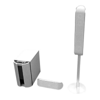
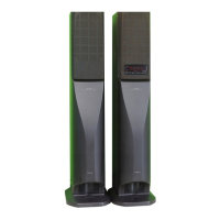
SA-SC8/WS8/SS-CT8/TS8
4
Note on Schematic Diagram:
• All capacitors are in µF unless otherwise noted. pF: µµF
50 WV or less are not indicated except for electrolytics
and tantalums.
• All resistors are in Ω and
1
/
4
W or less unless otherwise
specified.
• 2 : nonflammable resistor.
• 5 : fusible resistor.
• C : panel designation.
Note:
The components identi-
fied by mark 0 or dotted
line with mark 0 are criti-
cal for safety.
Replace only with part
number specified.
Note:
Les composants identifiés par
une marque 0 sont critiques
pour la sécurité.
Ne les remplacer que par une
piéce portant le numéro
spécifié.
• A : B+ Line.
• B : B– Line.
•Voltage is dc with respect to ground under no-signal
(detuned) condition.
•Voltages are taken with a VOM (Input impedance 10 MΩ).
Voltage variations may be noted due to normal produc-
tion tolerances.
• Signal path.
F : AUDIO
•Abbreviation
CND : Canadian model.
Note on Printed Wiring Boards:
• X : parts extracted from the component side.
• : Pattern from the side which enables seeing.
Ref. No. Location
D201 I-4
D202 H-4
D303 E-3
D304 E-3
D305 F-6
D306 D-8
D501 C-8
D502 E-8
D503 E-8
D504 E-8
D505 E-8
D506 F-7
D507 E-7
D601 I-7
D602 I-7
D603 J-7
D604 I-7
D605 H-7
D606 G-7
(D607) J-9
<D608> G-8
D701 B-5
D702 C-5
D703 C-5
D704 C-5
D801 E-10
IC101 C-3
IC102 C-2
IC104 C-5
IC201 H-3
IC202 H-1
IC203 H-3
IC204 H-4
IC301 E-2
IC701 B-6
Q101 C-1
Q301 E-3
Q302 E-2
Q303 E-2
Q304 D-2
Q305 D-3
Q306 D-3
Q307 D-3
Q308 E-7
Q309 F-6
Q310 E-6
Q311 E-6
Q401 J-3
Q402 J-3
Q403 J-2
Q404 J-5
Q501 F-7
Q502 E-7
Q601 H-7
Q602 G-7
Q701 B-5
Q702 C-6
Q703 A-7
Q704 A-7
Q705 A-7
• Semiconductor
Location
(): Except E model
<>: E model