77
STR-KSL7/SL7/TA-KSL7
SECTION 3
DIAGRAMS
For schematic diagrams.
Note:
• All capacitors are in µF unless otherwise noted. p : pF. 50
WV or less are not indicated except for electrolytics and
tantalums.
• All resistors are in Ω and
1
/
4
W or less unless otherwise
specified.
• % : indicates tolerance.
•
f
: internal component.
• C : panel designation.
• A : B+ Line.
• B : B– Line.
• Voltages and waveforms are dc with respect to ground
under no-signal (detuned) conditions.
No mark : FM
• Voltages are taken with a VOM (Input impedance 10 MΩ).
Voltage variations may be noted due to normal produc-
tion tolerances.
• Waveforms are taken with a oscilloscope.
• Circled numbers refer to waveforms.
• Signal path.
F : ANALOG
J : DIGITAL
c : DVD
• Abbreviation
CND : Canadian model
MY : Malaysia model
SP : Singapore model
CH : Chinese model
MX : Mexican model
THIS NOTE IS COMMON FOR PRINTED WIRING BOARDS AND SCHEMATIC DIAGRAMS.
(In addition to this necessary note is printed in each block.)
Note:
The components identified by
mark 0 or dotted line with mark
0 are critical for safety.
Replace only with part number
specified.
Note:
Les composants identifiés par
une marque 0 sont critiques
pour la sécurité.
Ne les remplacer que par une
pièce portant le numéro spécifié.
C
B
These are omitted.
E
Q
B
These are omitted.
CE
For printed wiring boards.
Note:
• X : parts extracted from the component side.
•
a
: Through hole.
•
f
: internal component.
• : Pattern from the side which enables seeing.
Caution:
Pattern face side: Parts on the pattern face side seen from
(Side A) the pattern face are indicated.
Parts face side: Parts on the parts face side seen from
(Side B) the parts face are indicated.
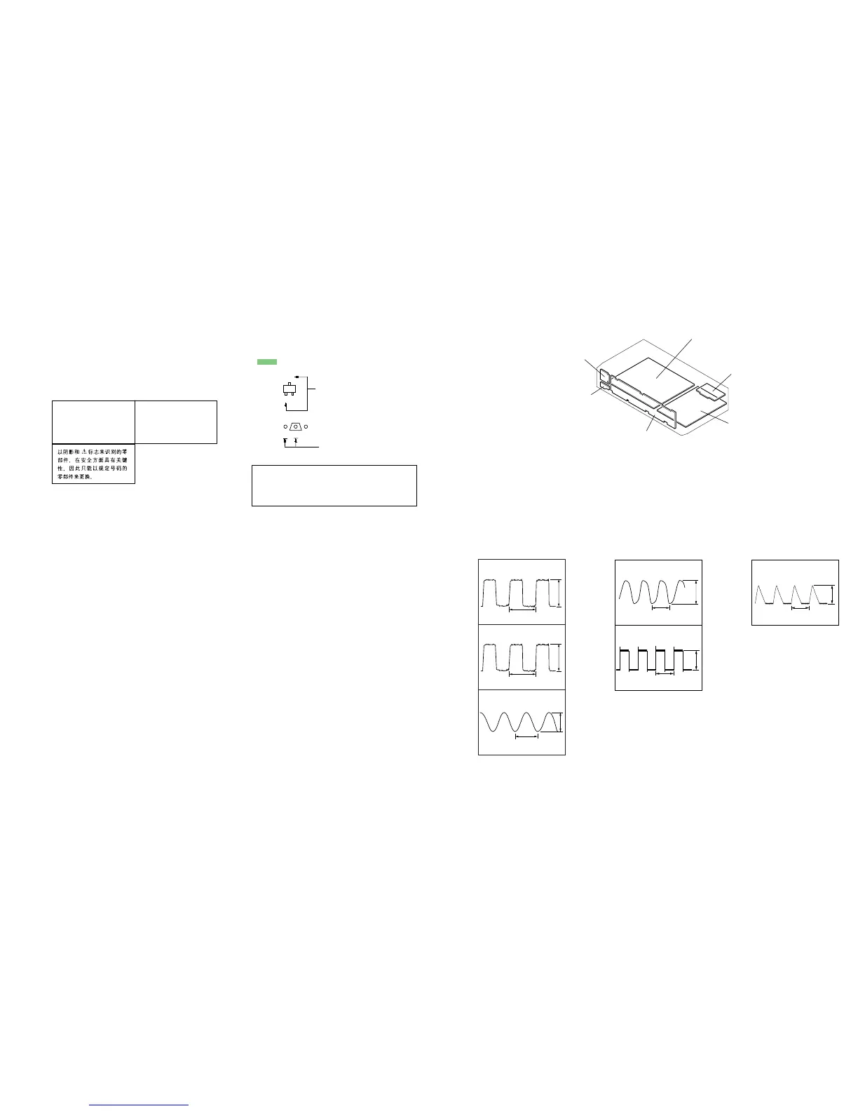
• CIRCUIT BOARDS LOCATION
• WAVEFORMS
– DIGITAL BOARD – – MAIN BOARD – – DISPLAY BOARD –
1
IC506 5
2
IC701 9
3
IC101 id
6Vp-p
81ns
20ns/div 2V/div
6.3Vp-p
81ns
20ns/div 2V/div
5.8Vp-p
62ns
20ns/div 2V/div
5Vp-p
1.3
µ
s
400ns/div 2V/div
4
IC306 4
5
IC309 wf
7.8Vp-p
20.3ns
10ns/div 2V/div
25.4Vp-p
9.8
µ
s
4
µ
s/div 10V/div
6 Q153 collector
HEADPHONE board
POWER SW board
MAIN board
DIGITAL board
S VIDEO board
DISPLAY board
• MAIN board consists of multiple layers.
However, only the sides (layers) A and B are shown.
 Loading...