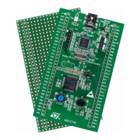
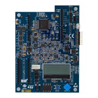
The STM32F0DISCOVERY is an evaluation and development kit designed to help users discover the features of the STM32 F0 Cortex™-M0 microcontroller and easily develop applications. It is based on the STM32F051R8T6, a 32-bit ARM® Cortex™ microcontroller from the STM32 F0 series.
Function Description
The kit provides a comprehensive platform for microcontroller development, integrating an ST-LINK/V2 embedded debug tool, user interface elements like LEDs and push buttons, and a prototyping board for custom extensions. It allows users to program and debug the on-board STM32 F0 microcontroller or an external STM32 application. The prototyping board supports various accessory modules, including Mikroelektronika "Click boards," ST MEMS adapter boards, and Arduino shield boards, enabling a wide range of application development.
Important Technical Specifications
Microcontroller:
The core of the STM32F0DISCOVERY is the STM32F051R8T6 microcontroller. This is a 32-bit low- and medium-density advanced ARM® Cortex™-M0 MCU with a high-performance ARM Cortex™-M0 32-bit RISC core.
- Flash Memory: 64 Kbytes
- RAM: 8 Kbytes
- Package: 64-pin LQFP
- CPU Frequency: Up to 48 MHz
- Voltage Supply: 1.8 V to 3.6 V
- Communication Interfaces:
- 18 Mbit/s SPI with 4- to 16-bit data frame
- 1 Mbit/s I²C fast-mode plus
- HDMI CEC
- USART
- Timers:
- 1x 16-bit 3-phase PWM motor control timer
- 5x 16-bit PWM timers
- 1x 16-bit basic timer
- 1x 32-bit PWM timer
- 12 MHz I/O toggling
- Analog Peripherals:
- 1x 12-bit ADC (up to 16 inputs)
- 2x Comparators
- 1x 12-bit DAC
Power Supply:
The board can be powered either via the host PC through a USB cable or by an external 5V power supply.
- Output Power Supplies: 5V and 3V pins can deliver power to external application boards, with consumption limited to less than 100 mA.
- Input Power Supplies: The 5V pin can also be used as an input. When using an external power supply unit, it must comply with EN-60950-1:2006+A11/2009 and be Safety Extra Low Voltage (SELV) with limited power capability.
Clocks:
- HSE Oscillator: PF0 and PF1 can be used as GPIO or as HSE oscillator. By default, they are configured as GPIO. An external HSE clock can be provided from the ST-LINK's MCO (fixed at 8 MHz) or an onboard X2 crystal (not provided), or an external oscillator through pin 7 of the P1 connector.
- LSE Oscillator: PC14 and PC15 can be used as GPIO or as LSE oscillator. By default, they are configured as GPIO. An external LSE clock can be provided from an onboard X3 crystal (not provided) or an external oscillator through pin 5 of the P1 connector.
Debug Tool:
- Embedded ST-LINK/V2: Supports Serial Wire Debug (SWD) for STM32 devices. It can be used for on-board programming/debugging or for external STM32 applications via the CN3 connector.
Usage Features
Getting Started:
- Verify jumper positions (JP2, CN2, CN1).
- Connect the board to a PC via a USB cable (Type A to mini-B) to power the board. LD1 (PWR) and LD2 (COM) LEDs will light up.
- Press user button B1 (bottom left corner of the board).
- Observe LD3 and LD4 LEDs changing according to user button B1 clicks.
- Each click on B1 confirms the blue LED LD4.
- Access www.st.com/stm32f0discovery for projects, tutorials, and documentation.
- Discover STM32F0 features, download and execute programs.
- Develop custom applications.
LEDs:
- LD1 (PWR): Red LED, indicates board power.
- LD2 (COM): Tricolor LED, indicates communication status:
- Slow blinking Red: Power on, before USB initialization.
- Fast blinking Red: First correct communication between PC and STLINK/V2.
- Red On: Initialization between PC and ST-LINK/V2 successful.
- Green On: Successful target communication initialization.
- Blinking Red/Green: During communication with target.
- Red On: Communication finished and OK.
- Orange On: Communication failure.
- LD3 (User): Green LED connected to I/O PC9 of STM32F051R8T6.
- LD4 (User): Blue LED connected to I/O PC8 of STM32F051R8T6.
Push Buttons:
- B1 (USER): User push button connected to I/O PA0 of STM32F051R8T6.
- B2 (RESET): Push button to reset the STM32F051R8T6.
Extension Connectors (P1 and P2):
Male headers P1 and P2 allow connection to standard prototyping/wrapping boards. STM32F051R8T6 GPIOs are available on these connectors and can be probed by an oscilloscope, logic analyzer, or voltmeter.
Prototyping Board Connectivity:
The kit supports various modules via its prototyping board:
- Mikroelektronika Accessory Boards (mikroBUS™ and IDC10):
- mikroBUS™: A 16-pin connector for SPI, USART, or I²C communications, with additional pins for Analog Input, PWM, and Interrupt. Compatible with "Click boards."
- IDC10: A 10-pin connector for general-purpose I/O.
- ST MEMS "Adapter Boards" (standard DIL24 socket): Allows connection of ST MEMS adapter boards for various sensors.
- Arduino Shield Boards: Compatible with Arduino shields, providing a broad range of expansion possibilities.
Maintenance Features
Jumper and Solder Bridge Settings:
The board includes various jumpers and solder bridges to configure the device's operation and connectivity.
- CN2 Jumpers:
- ON (default): ST-LINK/V2 functions enabled for on-board programming.
- OFF: ST-LINK/V2 functions enabled for external application via CN3.
- JP2 (Idd):
- ON (default): STM32F051R8T6 is powered.
- OFF: Allows measurement of STM32F051R8T6 current consumption by connecting an ammeter. If no ammeter is connected, the MCU will not be powered.
- Solder Bridges (SBx):
- SB16,17 (X2 crystal): OFF for external clock from P1, ON for X2 crystal.
- SB18 (MCO): ON provides 8 MHz from ST-LINK/V2 MCO for OSC_IN.
- SB20,21 (X3 crystal): OFF for external clock from P1, ON for X3 crystal.
- SB4 (B2-RESET): ON connects B2 push button to NRST pin of MCU.
- SB3 (B1-USER): ON connects B1 push button to PA0.
- SB1 (VBAT powered from VDD): ON powers VBAT from VDD.
- SB19 (NRST): ON connects NRST signal of CN3 to MCU NRST.
- SB22 (T_SWO): ON connects SWO signal of CN3 to PB3.
- SB13 (STM_RST): ON connects STM32F103C8T6 NRST to GND.
- SB2 (BOOTO): ON holds BOOTO low via a 510 Ohm pull-down resistor.
These configurations allow for flexible setup, enabling different clock sources, power measurement, and debugging scenarios, which are crucial for troubleshooting and optimizing applications.