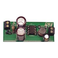
Circuit operation AN2544
4/17
1 Circuit operation
1.1 Input line rectification and line conducted filter
The circuit operations for all four versions are basically the same. The difference is in the
circuit for startup. Version 1 will be described here with reference to Figure 3. The output of
the converter is not isolated from the input. This makes neutral common to output ground
thus giving a reference back to neutral. The buck is less expensive due to the fact that it
does not use a transformer and an opto coupler. The AC line is applied through D1 which
rectifies the line input every other half cycle.
C1, L0, C2 form a pie filter to reduce EMI noise. The value of the capacitor is chosen to
maintain a reasonable valley, because the caps are charged every other half cycle. Two
diodes can be used in place of D1 to sustain burst pulses of 2 kV. R10 serves two purposes,
one is for inrush limiting and the other is to act as a fuse in case of a catastrophic failure. A
wire wound resistor handles the energy of the inrush. Flame proof resistor and a fuse can be
used depending on system and safety requirements. C7 helps the EMI by balancing line and
neutral noise without using an Xcap. This will pass EN55022 level "B". If the requirement is
less, then this cap can be left out of the circuit.
1.2 Start circuit
The voltage across C2 is fed to the drain, pin 5 through 8. Inside the VIPer, the constant
current source delivers 1mA to the V
dd
pin 4. This current charges C3. When the voltage on
the V
dd
pin reaches 14.5 V nominal, the current source turns off and the VIPer starts
pulsing. During this time, the energy is being supplied from the V
dd
cap. The energy stored
must be greater than the energy needed to supply the output current plus the energy to
charge of the output capacitor, before the V
dd
cap falls below 9 V. This can be seen in
Figure 8 and Figure 9. The value of the capacitor is therefore chosen to accommodate the
startup time. During a short circuit, the V
dd
cap discharges below the minim value enabling
the internal high voltage current generator to initiate a new startup sequence. The charging
and discharging of the capacitor determine the time period that the power supply is to be on
and off. This reduces the RMS heating effect on all components. The regulation circuit
consists of Dz, C4 and D8. D8 peak charges C4 during the freewheeling time when D5 is
conducting. During this time, the source or reference to the VIPer is one diode drop below
ground, which compensates for the D8 drop. So basically the Zener voltage is the same as
the output voltage. C4 is connected across V
fb
and source to filter the regulation voltage. Dz
is a BZT52C12, ½ W Zener with a specified test current of 5 mA. These Zeners that are
specified at a lower current give better accuracy of the output voltage. If the output voltage is
lower than 16 V, the circuit can be configured as in Figure 3 where V
dd
is separated from the
V
fb
pin. When the internal current source charges the V
dd
cap, V
dd
can reach 16V at worse
case condition. A 16 V Zener with a 5% low tolerance can be 15.2 V plus the internal
resistance to ground is 1230 Ω which is an additional 1.23 V for a total of 16.4 V. For 16 V
output and higher, the V
dd
pin and the V
fb
pin can share a common diode and capacitor filter
similar to Figure 4.