RT-9000C Hardware Supplement
Document No. 8121000602
Revision A (19 Mar 2007)
8-23
RT-9000 C
8.3.2 Digital IF & Audio Board Set
8.3.2.1 Description
The RT-9000C Transceiver uses redesigned versions of earlier analog IF 1A2A4 and Audio 1A2A3
assemblies. The new assemblies are digital designs and are, in fact, what sets the RT-9000C transceiver
apart from its predecessors. These new assemblies are designed to be backward compatible with previously
produced RT-9000 transceiver models. Due to the design implementation, however, these two assemblies
can ONLY operate as a pair. Each new digital assembly type CANNOT replace its earlier analog counterpart
by itself. The new two-board set together, however, fully replaces the combined functions of the original
analog IF and Audio assemblies.
This qualified interchangeability situation will never be a problem with the RT-9000C Transceivers since they
will always use the new digital two-board set. Use and application of the new two-board set in earlier models
has not been fully defined or implemented as of this writing.
8.3.2.2 Theory of Operation
This section describes the theory of operation of the new digital two-board set in the RT-9000C Transceiver.
This explanation supplements the theory of operation described in Section 4 of the RT-9000 Operation &
Maintenance manual to which this supplement is attached. The theory of operation is described for receive-
state and transmit-state and supplements original manual sections 4.3 and 4.4, respectively. The theory of
operation explanation begins and ends at the Front End Assembly (1A2A5) – to - IF Assembly (1A2A4)
interconnection point.
8.3.2.2.1 Receive-State Operation
1A2A4 Digital IF Assembly
The 48.305 MHz First IF output from the 1A2A5 Front End Assembly enters the 1A2A4 Digital IF
Assembly at coaxial connector P4. The signal is switched through diode gate CR1 and routed to 48.305
MHz crystal filter FL1. The band-pass filtered signal is switched through diode gate CR4 and passes to
low-noise amplifier U1. The amplified signal from U1 is switched through diode gate CR5 and routed to
mixer X1. The signal is mixed with the Second Local Oscillator, which has a frequency of 47.85 MHz.
This produces the 455 kHz Second IF receive signal.
The 455 kHz signal is switched through diode gate CR23 and again amplified by U10. The signal is
switched by diode gate CR28 to transformer T4. The signal passes to T1, which splits it into two equal
amplitude signals. One signal is filtered by FL2, which is an LSB filter but used for USB reception
. The
other signal is filtered by FL3 or FL4. While FL3 is an USB filter it is used for LSB reception. The USB and
LSB signal frequencies are transposed due to the frequency conversion scheme used in this design.
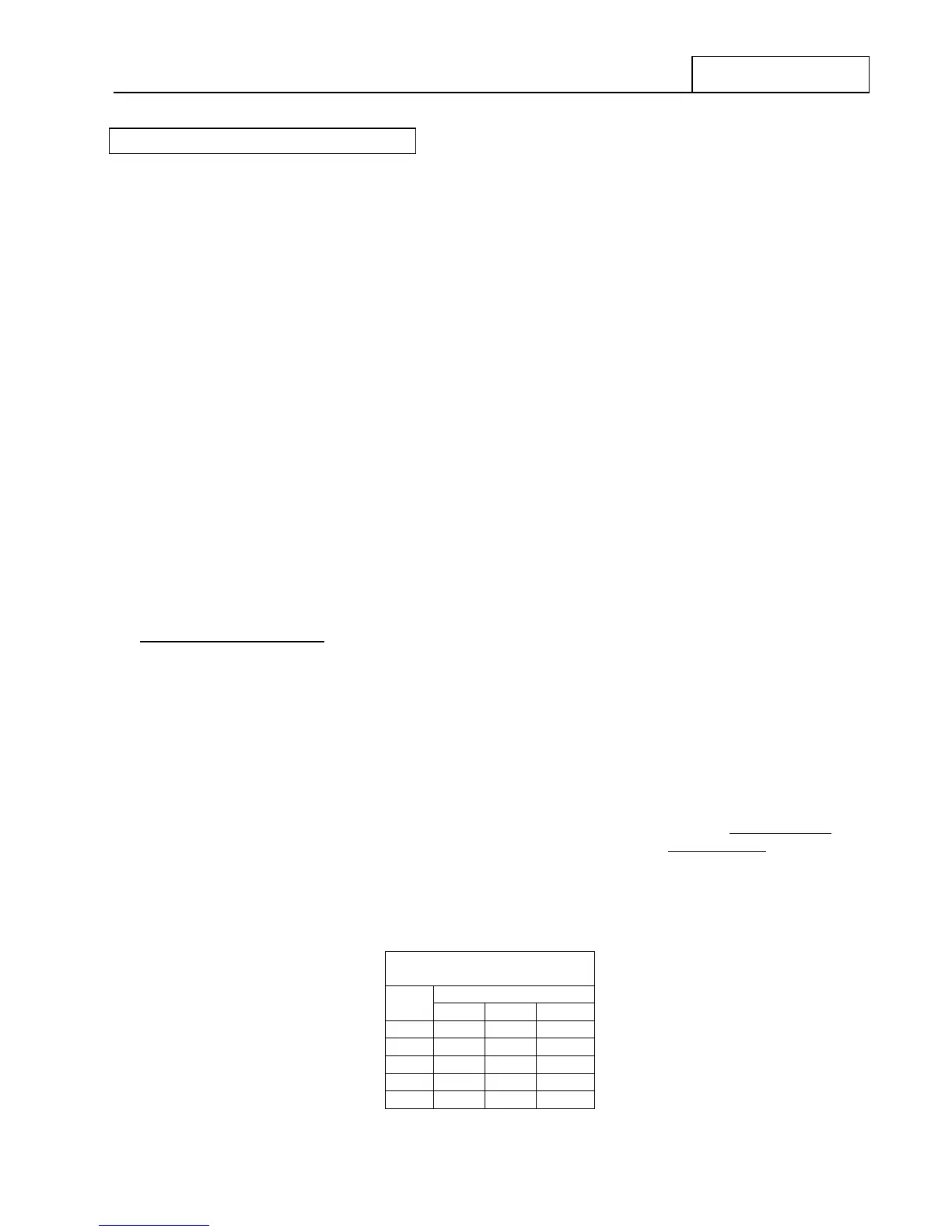
Refer to following table, which shows how these filter(s) are used when receiving various emission mode
signals. Note that this filter usage is somewhat different during transmit-state operation covered later.
Receive-State
Emission Mode vs. Filter Usage
455 kHz Filters
Mode
FL2 FL3 FL4
USB
X
LSB
X
AME
X
CW
X
ISB
X X
 Loading...