30
X11SSZ-TLN4F/QF/F User's Manual
2.4 Memory Support and Installation
Note: Check the Supermicro website for recommended memory modules.
Important: Exercise extreme care when installing or removing DIMM modules to pre-
vent any possible damage.
Memory Support
The X11SSZ-TLN4F/F supports up to 64GB of Unbuffered (UDIMM) DDR4 ECC/Non-ECC
2133 MHz in four memory slots. The X11SSZ-QF supports up to 64GB of Unbuffered (UDIMM)
DDR4 Non-ECC 2133 MHz in four memory slots. Populating these DIMM modules with a
pair of memory modules of the same type and size will result in interleaved memory, which
will improve memory performance.
Note: Be sure to use memory modules of the same type and speed on the motherboard.
Mixing of memory modules of different types and speeds is not allowed.
DIMM Module Population Conguration
For optimal memory performance, follow the table below when populating memory.
Recommended Population (Balanced)
DIMMA1 DIMMB1 DIMMA2 DIMMB2 Total System Memory
2GB 2GB 4GB
2GB 2GB 2GB 2GB 8GB
4GB 4GB 8GB
4GB 4GB 4GB 4GB 16GB
8GB 8GB 16GB
8GB 8GB 8GB 8GB 32GB
16GB 16GB 32GB
16GB 16GB 16GB 16GB 64GB
DIMMB2 (Blue Slot)
DIMMA2 (Blue Slot)
Towards the edge of the motherboard
Towards the CPU
DIMMA1
DIMMB1
DIMM Module Population Sequence
When installing memory modules, the DIMM slots must be populated in the following order:
DIMMB2, DIMMA2, then DIMMB1, DIMMA1. The blue slots must be populated rst.
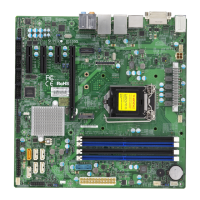
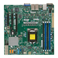
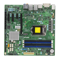
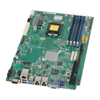
USB10/11(3.0)
AUDIO FP
PCH SLOT4 PCI-E 3.0 X4(IN X8)
CPU SLOT6 PCI-E 3.0 X16
PCH SLOT7 PCI-E 3.0 X4(IN X8)
DP1/DP2
VGA/DVI
LAN3/4
LAN1/2
USB2/3(3.0)
IPMI_LAN
USB0/1
1
1
1
1
1
1
1
1
1
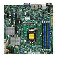
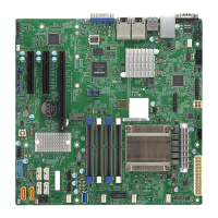
X11SSZ-F
REV: 1.10
MAC CODE
MAC CODE
MAC CODE
MAC CODE
MAC CODE
BAR CODE
DESIGNED IN USA
BIOS LICENSE
CPU Socket LGA1151
S/N CODE
Intel
C236
1
1
USB8/9
USB6/7
USB4/5
I-SGPIO1
JPW2
SP1
BT1
LED1
LED2
JD1
JBT1
JPI2C1
JGPIO1
FAN4
FAN2
FAN1
FANB
FANA
FAN3
JTPM1
JSPDIF_OUT1
JL1
J18
JI2C2
JI2C1
JPW1
JPME2
JBR2
JBR3
JPL3
JPL2
JPL1
JBR1
JWD1
JPB1
JPG1
JPAC1
COM2
COM1
LED4
LED3
JSD1
J15
DIMMA1
DIMMA2
DIMMB1
DIMMB2
JF1
I-SATA1
I-SATA2
I-SATA3
I-SATA0
JUIDB1
JIPMB1
JSMB1
1
1
1
JVR1
JVRM1
JVRM2
USB12
4
3
2
JPWR1
 Loading...