Theory of Operation-2225 Service
for minimal dc trace shift in CH 2 INVERT when
rotating CH
2
Variable VOLTSIDIV. Balance
Potentiometer R84 is switched in with R83 when in
NORM; it is adjusted for minimal dc trace shift when
rotating CH 2 Variable VOLTSIDIV.
Vertical Preamplifiers
The Channel 1 and Channel 2 Vertical Preamplifiers,
shown on diagram 2, are identical in operation.
Operation of the Channel 1 amplifier is described.
Differential signal current from the Paraphase Ampli-
fier is amplified to produce drive current for the
Delay Line Driver. Internal trigger signals for the
Trigger circuitry are picked off prior to the Vertical
Preamplifier. The Channel Switch circuitry controls
channel selection for the crt display.
Common-base transistors Q102 and
(2103, which
complete the Paraphase Amplifier portion of the
circuitry shown on diagram 1, convert differential
current from the Paraphase Amplifier into level-
shifted voltages that drive the bases of the input
transistors of Vertical Preamplifier U130 and the
Internal Trigger circuitry.
Common-mode components
CR104, CR105, R104,
and R105 provide XI gain. XI0 gain is selected by
switching in
CR111, CR112, R107, R110, R111,
R112, and R128. XlO gain is adjusted by R112, and
XI0 balance is set by R107. C110 limits the
bandwidth in
XI0 mode to about 5.2 MHz to
7.8
MHz.
Emitter current for the input transistors of U130 is
supplied by
Q114 and Q115. The base bias voltage
to
Q114 and Q115 is unbalanced through poten-
tiometer R123 (the CH 1 POSITION control) to pro-
duce vertical positioning of the Channel 1 trace. The
collector current of each input transistor of U130 is
the emitter current for two of the differential output
transistors. One of the collectors of each output pair
is grounded, and the other provides output drive to
the Delay Line Driver. The base bias voltages of the
transistors with grounded collectors are held at
ground potential by
R136. The base voltages of the
other transistors are controlled by the Channel
Switch circuitry.
When Channel
1
is selected to drive the Delay Line
Driver, the
Q
output (pin
9)
of U540A is HI. The tran-
sistors with the ungrounded collectors are then
forward-biased, and the Channel 1 signal is con-
ducted through to the Delay Line Driver. If Channel 1
is not selected, then the
Q
output of U540A is
LO.
The transistors with the ungrounded collectors are
then reverse-biased, and the output signals will be
conducted to ground by the other transistor pair.
The gain of the Preamplifier is set by adjusting
R145
to control the signal current that is shunted between
the two differential outputs.
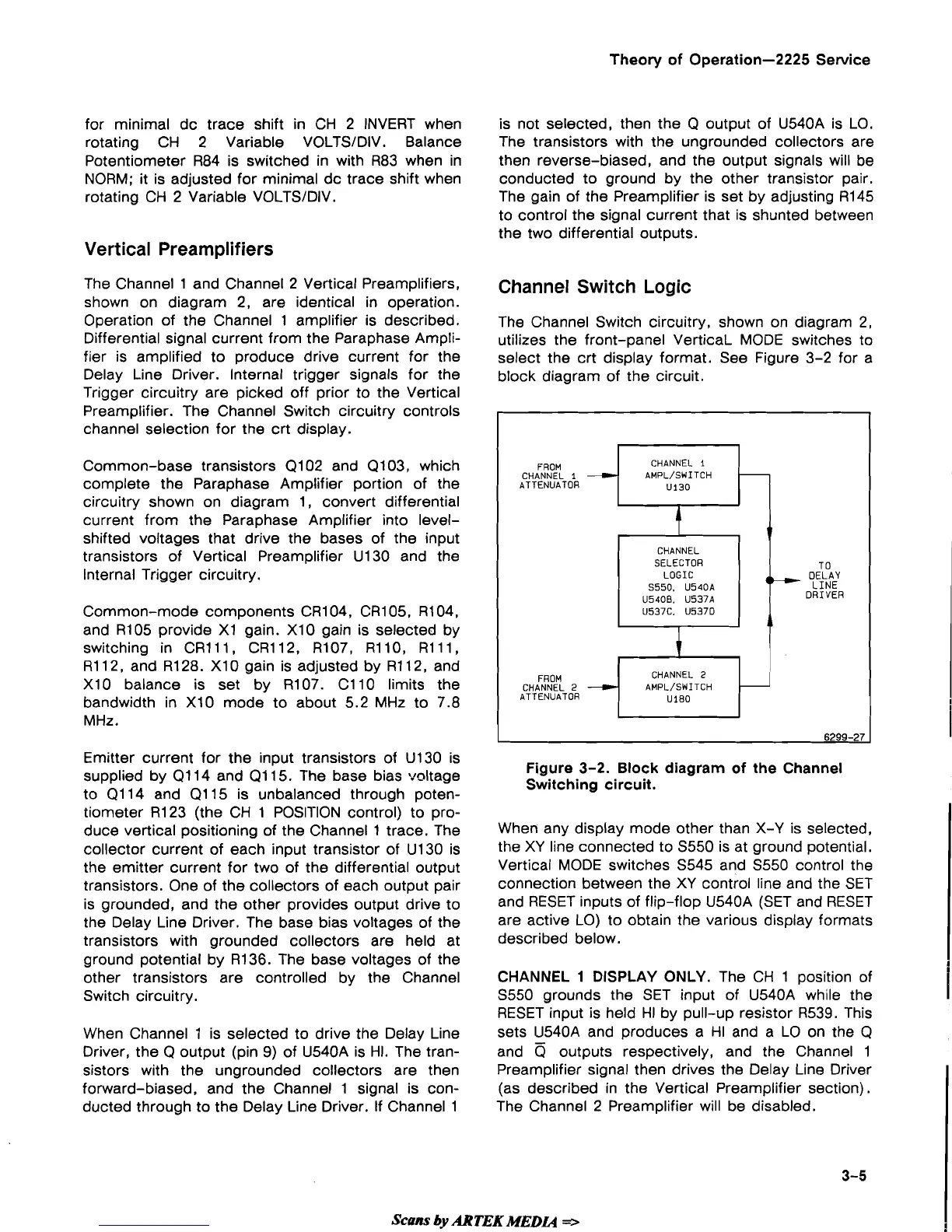
Channel Switch Logic
The Channel Switch circuitry, shown on diagram 2,
utilizes the front-panel
VerticaL MODE switches to
select the crt display format. See Figure 3-2 for a
block diagram of the circuit.
Figure
3-2.
Block diagram
of
the Channel
Switching circuit.
FROM
CHANNEL
1
ATTENUATOR
When any display mode other than X-Y is selected,
the XY line connected to S550 is at ground potential.
Vertical MODE switches S545 and S550 control the
connection between the XY control line and the SET
and RESET inputs of flip-flop
U540A (SET and RESET
are active LO) to obtain the various display formats
described below.
CHANNEL
1
DISPLAY ONLY.
The CH 1 position of
S550 grounds the SET input of
U540A while the
RESET input is held HI by pull-up resistor
R539. This
sets
U540A and produces a HI and a
LO
on the Q
and
a
outputs respectively, and the Channel 1
Preamplifier signal then drives the Delay Line Driver
(as described in the Vertical Preamplifier section).
The Channel 2 Preamplifier will be disabled.
CHANNEL
1
AMPL/SWITCH
U130
Scans
by
ARTEK
MEDL4
*
-
'
T 0
,-
OELAY
LINE
DRIVER
I
t
1
CHANNEL
SELECTOR
LOGIC
5550. U540A
U540B. U537A
U537C. U537D
I
-
ATTENUATOR
FROM
CHANNEL
2
-
U180
CHANNEL
2
AMPL/SWITCH
6299-27
 Loading...