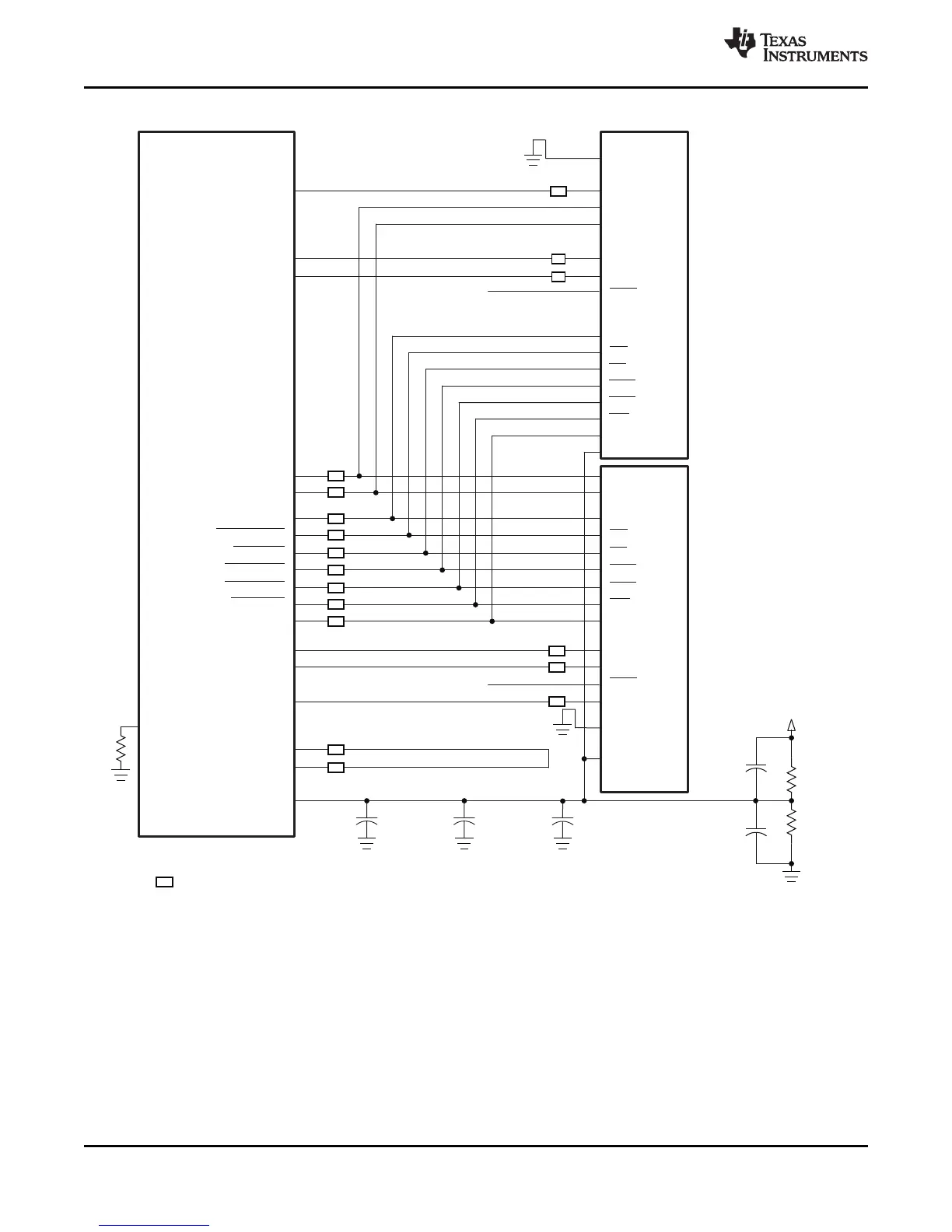
DDR2/mDDR Memory Controller
DDR_D[0:7]
Lower Byte
DDR2/mDDR
DDR_DQM[0]
DDR_DQS[0]
ODT
DQ0 - DQ7
BA0-BA2
CK
CK
DM
DQS
DQS
CS
CAS
RAS
DDR_BA[0:2]
CKE
BA0-BA2
DDR_A[0:13]
DDR_CLKP
A0-A13
DDR_CLKN
DDR_CS
CK
CS
DDR_CAS
DDR_RAS
CAS
RAS
DDR_WE
WE
DDR_D[8:15]
DQS
DQ0 - DQ7
DDR_DQGATE0
DDR_DQGATE1
T
T
T
T
T
T
T
T
T
T
T
T
T
T
DDR_ZP
VREF
(3)
DDR_VREF
1 K Ω 1%
DDR_DVDD18
VREF
1 K Ω 1%
0.1 μF
0.1 μF
0.1 μF
(2)
0.1 μF
(2)
0.1 μF
(2)
50 5Ω %
T
Terminator, if desired. See terminator comments.
ODT
A0-A13
WE
VREF
Upper Byte
DDR2/mDDR
CK
DDR_CKE
CKE
T
DDR_DQM1
DM
T
DDR_DQS1
DQS
T
NC
NC
(1)
AM1808
SPRS653E –FEBRUARY 2010–REVISED MARCH 2014
www.ti.com
(1) See Figure 6-23 for DQGATE routing specifications.
(2) For DDR2, one of these capacitors can be eliminated if the divider and its capacitors are placed near a device VREF pin. For mDDR,
these capacitors can be eliminated completely.
(3) VREF applies in the case of DDR2 memories. For mDDR, the DDR_VREF pin still needs to be connected to the divider circuit.
Figure 6-17. DDR2/mDDR Dual-Memory High Level Schematic
112 Peripheral Information and Electrical Specifications Copyright © 2010–2014, Texas Instruments Incorporated
Submit Documentation Feedback
Product Folder Links: AM1808