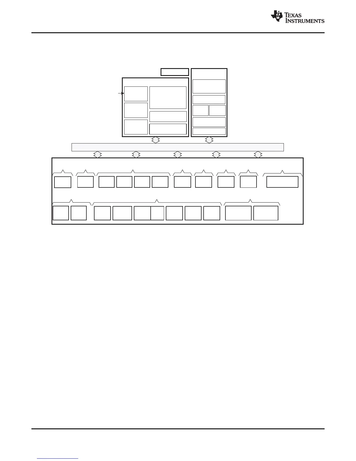
Switched Central Resource (SCR)
16KB
I-Cache
16KB
D-Cache
4KB ETB
ARM926EJ-S CPU
With MMU
ARM Subsystem
JTAG Interface
System Control
Input
Clock(s)
64KB ROM
8KB RAM
(Vector Table)
Power/Sleep
Controller
Pin
Multiplexing
PLL/Clock
Generator
w/OSC
General-
Purpose
Timer (x3)
Serial Interfaces
Audio Ports
McASP
w/FIFO
DMA
Peripherals
Display Internal Memory
LCD
Ctlr
128KB
RAM
External Memory InterfacesConnectivity
EDMA3
(x2)
Control Timers
ePWM
(x2)
eCAP
(x3)
EMIFA(8b/16B)
NAND/Flash
16b SDRAM
DDR2/MDDR
Controller
RTC/
32-kHz
OSC
I C
(x2)
2
SPI
(x2)
UART
(x3)
McBSP
(x2)
Video
VPIF
Parallel Port
uPP
EMAC
10/100
(MII/RMII)
MDIO
USB1.1
OHCI Ctlr
PHY
USB2.0
OTG Ctlr
PHY
HPI
MMC/SD
(8b)
(x2)
SATA
Customizable Interface
PRU Subsystem
Memory
Protection
AM1808
SPRS653E –FEBRUARY 2010–REVISED MARCH 2014
www.ti.com
1.4 Functional Block Diagram
Figure 1-1 shows the functional block diagram of the device.
(1) Note: Not all peripherals are available at the same time due to multiplexing.
Figure 1-1. Functional Block Diagram
4 AM1808 ARM Microprocessor Copyright © 2010–2014, Texas Instruments Incorporated
Submit Documentation Feedback
Product Folder Links: AM1808