AM1808
www.ti.com
SPRS653E –FEBRUARY 2010–REVISED MARCH 2014
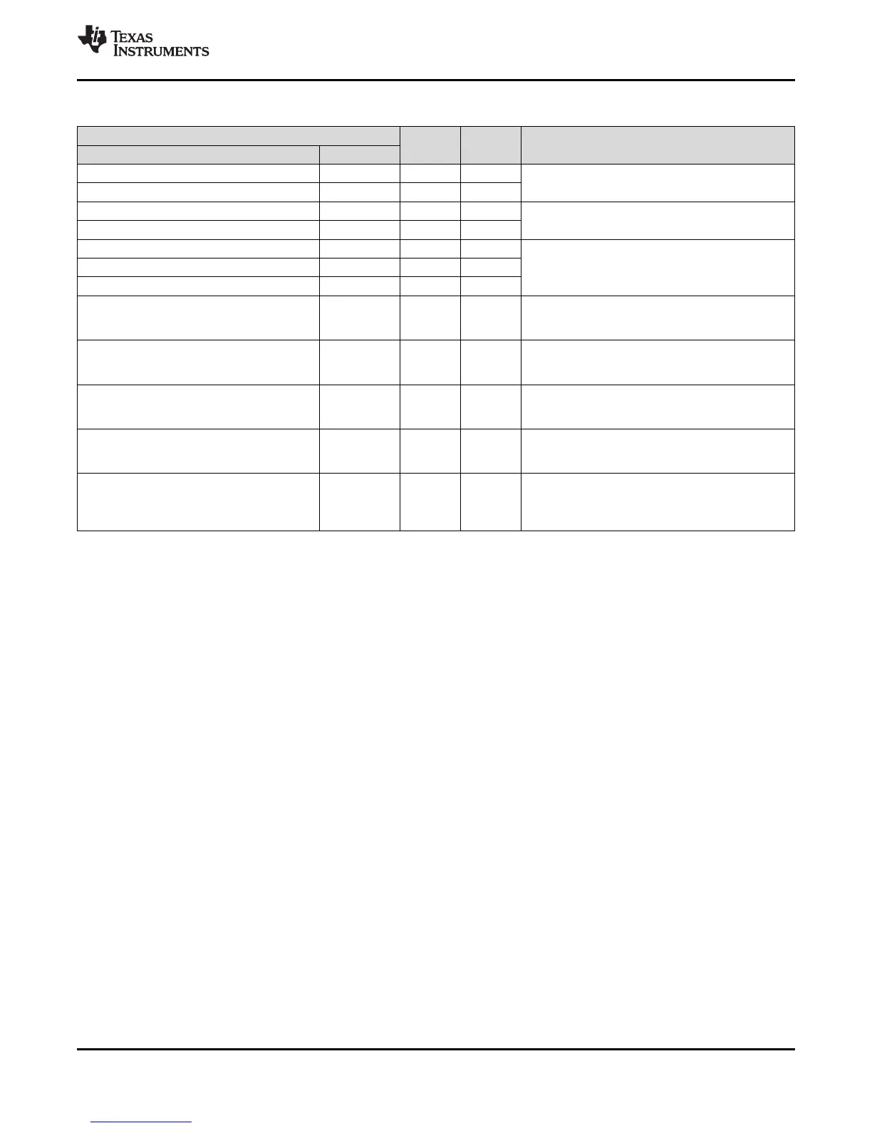
Table 3-8. DDR2/mDDR Terminal Functions (continued)
SIGNAL
TYPE
(1)
PULL
(2)
DESCRIPTION
NAME NO.
DDR_DQM[0] W13 O IPD
DDR2 data mask outputs
DDR_DQM[1] R10 O IPD
DDR_DQS[0] T14 I/O IPD
DDR2 data strobe inputs/outputs
DDR_DQS[1] V11 I/O IPD
DDR_BA[2] U8 O IPD
DDR_BA[1] T9 O IPD DDR2 SDRAM bank address
DDR_BA[0] V8 O IPD
DDR2 loopback signal for external DQS gating.
DDR_DQGATE0 R11 O IPD Route to DDR and back to DDR_DQGATE1 with
same constraints as used for DDR clock and data.
DDR2 loopback signal for external DQS gating.
DDR_DQGATE1 R12 I IPD Route to DDR and back to DDR_DQGATE0 with
same constraints as used for DDR clock and data.
DDR2 reference output for drive strength calibration
DDR_ZP U12 O — of N and P channel outputs. Tie to ground via 50
ohm resistor @ 5% tolerance.
DDR voltage input for the DDR2/mDDR I/O buffers.
DDR_VREF R6 I — Note even in the case of mDDR an external resistor
divider connected to this pin is necessary.
N10, P10, N9,
P9, R9, P8,
DDR_DVDD18 PWR — DDR PHY 1.8V power supply pins
R8, P7, R7,
N6
Copyright © 2010–2014, Texas Instruments Incorporated Device Overview 25
Submit Documentation Feedback
Product Folder Links: AM1808