MT8206
PRELIMINARY, SUBJECT TO CHANGE WITHOUT NOTICE MTK CONFIDENTIAL, NO DISCLOSURE
June, 2006
Refer to the Fig. 1-1 above. The dielectrics between conductors were as the isolators,
which were used to separate the conductors. By the microstrip line architecture of system
memory signals, the target impedance was desired to have 55 +/- 10%. Please refer to the
table 1 below for your PCB design and recommendation. The default design was 6-mil trace
width with 4.5 mil high dielectrics.
Table 1-1. 4 Layer PCB Stack up Configurations
PCB Parameter
H (mil)
Target Impedance (
)
Tolerance
5 4 55 10 %
6 4.5
55 10 %
Trace Width
(mil)
8 7 55 10 %
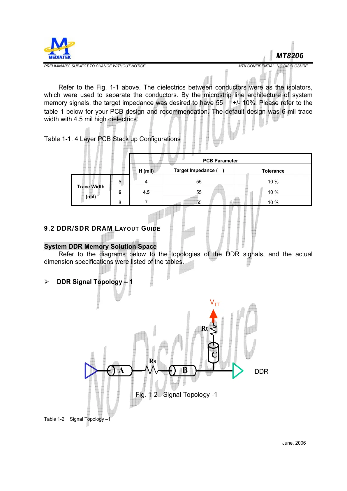
9.2 DDR/SDR DRAM LAYOU T GUIDE
System DDR Memory Solution Space
Refer to the diagrams below to the topologies of the DDR signals, and the actual
dimension specifications were listed of the tables.
¾ DDR Signal Topology – 1
Rs
Rt
Fig. 1-2 Signal Topology -1
DDR
V
TT
AB
C
Table 1-2. Signal Topology –1