MT8206
PRELIMINARY, SUBJECT TO CHANGE WITHOUT NOTICE MTK CONFIDENTIAL, NO DISCLOSURE
June, 2006
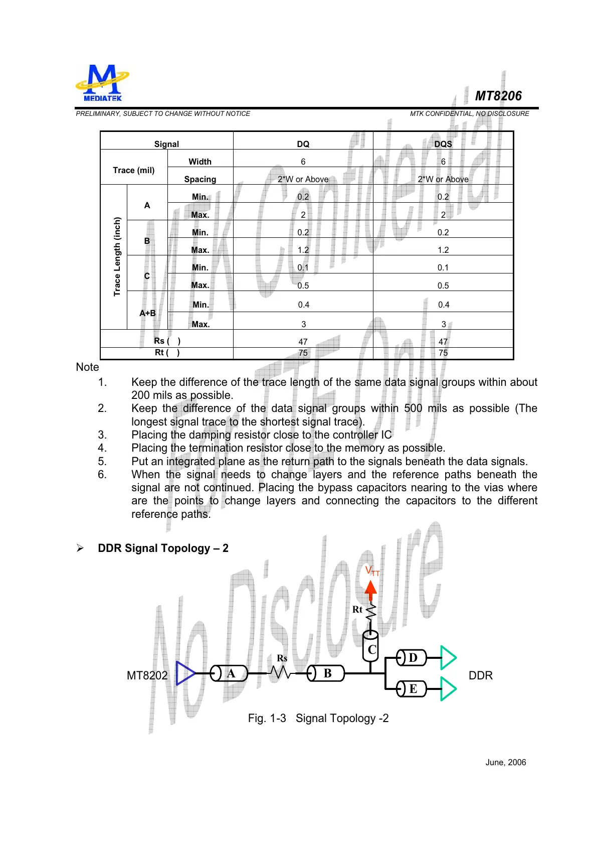
Rs
Rt
Fig. 1-3 Signal Topology -2
MT8202
V
TT
AB
C
D
E
DDR
Signal DQ DQS
Width 6 6
Trace (mil)
Spacing
2*W or Above 2*W or Above
Min.
0.2 0.2
A
Max.
2 2
Min.
0.2 0.2
B
Max.
1.2 1.2
Min.
0.1 0.1
C
Max.
0.5 0.5
Min.
0.4 0.4
Trace Length (inch)
A+B
Max.
3 3
Rs ( )
47 47
Rt ( )
75 75
Note
1. Keep the difference of the trace length of the same data signal groups within about
200 mils as possible.
2. Keep the difference of the data signal groups within 500 mils as possible (The
longest signal trace to the shortest signal trace).
3. Placing the damping resistor close to the controller IC
4. Placing the termination resistor close to the memory as possible.
5. Put an integrated plane as the return path to the signals beneath the data signals.
6. When the signal needs to change layers and the reference paths beneath the
signal are not continued. Placing the bypass capacitors nearing to the vias where
are the points to change layers and connecting the capacitors to the different
reference paths.
¾ DDR Signal Topology – 2