MT8206
PRELIMINARY, SUBJECT TO CHANGE WITHOUT NOTICE MTK CONFIDENTIAL, NO DISCLOSURE
June, 2006
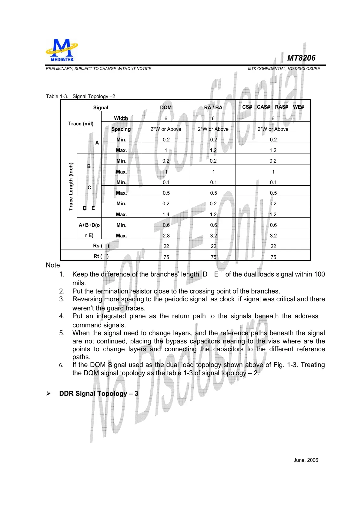
Table 1-3. Signal Topology –2
Signal DQM RA / BA
CS#
CAS# RAS# WE#
Width
6 6 6
Trace (mil)
Spacing
2*W or Above 2*W or Above 2*W or Above
Min.
0.2 0.2 0.2
A
Max.
1 1.2 1.2
Min.
0.2 0.2 0.2
B
Max.
1 1 1
Min.
0.1 0.1 0.1
C
Max.
0.5 0.5 0.5
Min.
0.2 0.2 0.2
D E
Max.
1.4 1.2 1.2
Min.
0.6 0.6 0.6
Trace Length (inch)
A+B+D(o
r E)
Max.
2.8 3.2 3.2
Rs ( )
22 22 22
Rt ( )
75 75 75
Note
1. Keep the difference of the branches’ length D E of the dual loads signal within 100
mils.
2. Put the termination resistor close to the crossing point of the branches.
3. Reversing more spacing to the periodic signal as clock if signal was critical and there
weren’t the guard traces.
4. Put an integrated plane as the return path to the signals beneath the address
command signals.
5. When the signal need to change layers, and the reference paths beneath the signal
are not continued, placing the bypass capacitors nearing to the vias where are the
points to change layers and connecting the capacitors to the different reference
paths.
6. If the DQM Signal used as the dual load topology shown above of Fig. 1-3. Treating
the DQM signal topology as the table 1-3 of signal topology – 2.
¾ DDR Signal Topology – 3