MT8206
PRELIMINARY, SUBJECT TO CHANGE WITHOUT NOTICE MTK CONFIDENTIAL, NO DISCLOSURE
June, 2006
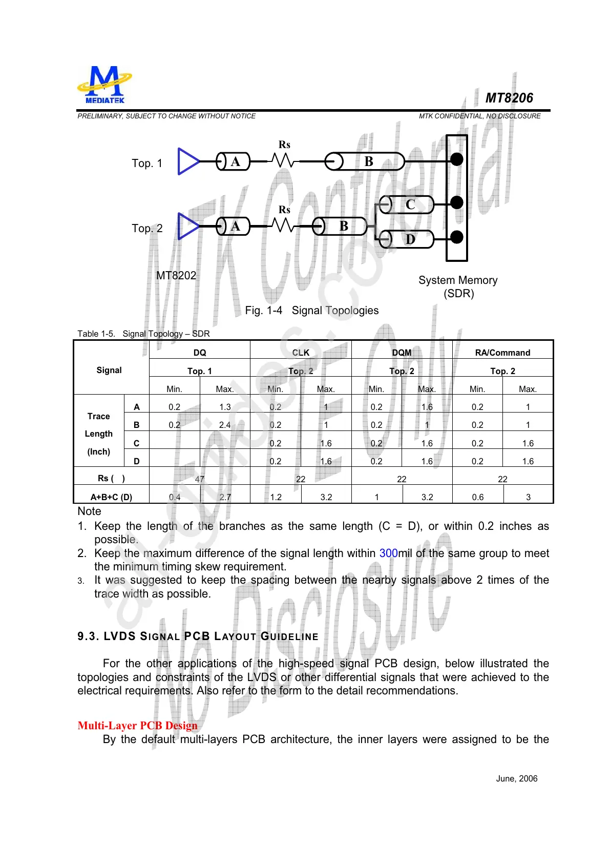
Fig. 1-4 Signal Topologies
System Memory
(SDR)
MT8202
Rs
Top. 1
AB
Rs
A B
C
D
Top. 2
Table 1-5. Signal Topology – SDR
DQ CLK DQM RA/Command
Top. 1 Top. 2 Top. 2 Top. 2
Signal
Min. Max. Min. Max. Min. Max. Min. Max.
A
0.2 1.3 0.2 1 0.2 1.6 0.2 1
B
0.2 2.4 0.2 1 0.2 1 0.2 1
C
0.2 1.6 0.2 1.6 0.2 1.6
Trace
Length
(Inch)
D
0.2 1.6 0.2 1.6 0.2 1.6
Rs ( )
47 22 22 22
A+B+C (D)
0.4 2.7 1.2 3.2 1 3.2 0.6 3
Note
1. Keep the length of the branches as the same length (C = D), or within 0.2 inches as
possible.
2. Keep the maximum difference of the signal length within 300mil of the same group to meet
the minimum timing skew requirement.
3. It was suggested to keep the spacing between the nearby signals above 2 times of the
trace width as possible.
9.3. LVDS SIGNAL PCB LAY O UT GUIDELINE
For the other applications of the high-speed signal PCB design, below illustrated the
topologies and constraints of the LVDS or other differential signals that were achieved to the
electrical requirements. Also refer to the form to the detail recommendations.
Multi-Layer PCB Design
By the default multi-layers PCB architecture, the inner layers were assigned to be the