MT8206
PRELIMINARY, SUBJECT TO CHANGE WITHOUT NOTICE MTK CONFIDENTIAL, NO DISCLOSURE
June, 2006
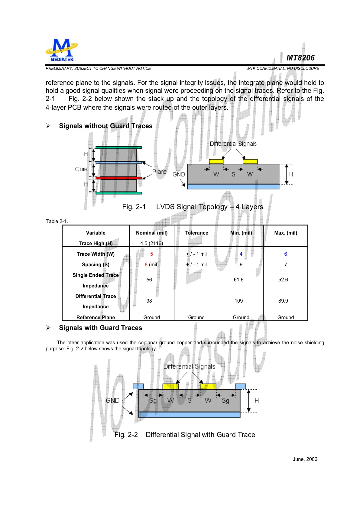
reference plane to the signals. For the signal integrity issues, the integrate plane would held to
hold a good signal qualities when signal were proceeding on the signal traces. Refer to the Fig.
2-1 Fig. 2-2 below shown the stack up and the topology of the differential signals of the
4-layer PCB where the signals were routed of the outer layers.
¾ Signals without Guard Traces
Fig. 2-1 LVDS Signal Topology – 4 Layers
Table 2-1.
Variable Nominal (mil) Tolerance Min. (mil) Max. (mil)
Trace High (H)
4.5 (2116)
Trace Width (W)
5 + / - 1 mil 4 6
Spacing (S)
8 (mil) + / - 1 mil 9 7
Single Ended Trace
Impedance
56 61.6 52.6
Differential Trace
Impedance
98 109 89.9
Reference Plane
Ground Ground Ground Ground
¾ Signals with Guard Traces
The other application was used the coplanar ground copper and surrounded the signals to achieve the noise shielding
purpose. Fig. 2-2 below shows the signal topology.
Fig. 2-2 Differential Signal with Guard Trace