SECTION
3
CIRCUIT DESCRIPTION
GENERAL DESCRIPTION
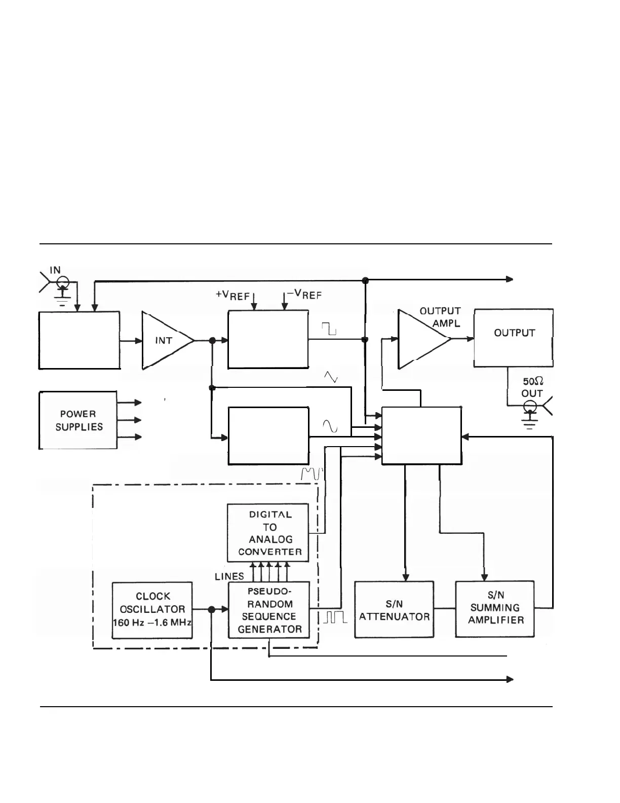
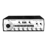
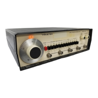
Refer to the block diagram of the Model 132
VCG/
Noise Generator, Figure 3-l.
Basically, a square wave is applied to the input of an
integrator composed of a wide-band differential dc
amplifier, integrating resistor and capacitor. Output
of the integrator is fed into the hysteresis switch.
The hysteresis and output switches function like a
Schmitt trigger with the limit points set at the
wave-
form extremes, firing when the triangle wave reaches
+1.25
volts and -1.25 volts. When firing occurs, the
hysteresis and output switches are set, reversing the
square wave fed into the integrator. Reversal of the
square wave causes the triangle wave to reverse direc-
VCG
VCG
Cl RCUIT
+5
v
POWER
SUPPLIES
+15 v
-15 v
HYSTERESIS
OUTPUT
SWITCH
ATTENUATOR
I
MODE
SINE
CONVERTER
SWITCHING
CIRCUIT
FUNC
SYNC
OUT
DIGITAL
I
I
FILTER
I
I
I
23
NOISE
SYNC
NOISE
CLOCK
Figure 3-l. Functional Block Diagram
11