EasyManua.ls Logo

Yamaha PORTATONE PSR-170 User Manual

Yamaha PORTATONE PSR-170
26 pages
To Next Page IconTo Next Page
Page #1 background imageLoading...
Page #1 background image
SERVICE MANUAL
CONTENTS
SPECIFICATIONS.............................................................................. 3
PANEL LAYOUT ................................................................................. 4
BLOCK DIAGRAM ............................................................................. 5
CIRCUIT BOARD LAYOUT & WIRING .............................................. 6
DISASSEMBLY PROCEDURE .......................................................... 7
LSI PIN DESCRIPTION ................................................................... 10
IC BLOCK DIAGRAM....................................................................... 11
CIRCUIT BOARDS .......................................................................... 12
TEST PROGRAM ............................................................................ 15
MIDI IMPLEMENTATION CHART .................................................... 17
OVERALL CIRCUIT DIAGRAM
PARTS LIST
This document is printed on chlorine free (ECF) paper with soy ink.
1.412K-355 Printed in Japan ’01.05
PK 001652
www.freeservicemanuals.info
3/24/2019
Digitized in Heiloo the Netherlands
Not for sale!
Question and Answer IconNeed help?

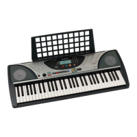
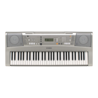
Do you have a question about the Yamaha PORTATONE PSR-170 and is the answer not in the manual?
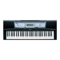
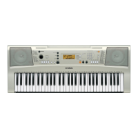
Yamaha PORTATONE PSR-170 Specifications

General IconGeneral
Keyboard61 keys
Voices100
Styles100
Songs100
MIDIYes
EffectsReverb, Chorus
Power SupplyPA-3B adapter or batteries
DisplayLCD
ConnectionsDC IN
Weight4.5 kg
Amplifier2.5W x 2

Summary

SPECIFICATIONS

PANEL LAYOUT

Top Panel

Overview of controls and indicators on the keyboard's top surface.

Rear Panel

Details of connectors and ports located on the rear of the keyboard.

BLOCK DIAGRAM

CIRCUIT BOARD LAYOUT & WIRING

Upper case side

Component and connector placement on the upper chassis.

Lower case side

Component and connector placement on the lower chassis.

DISASSEMBLY PROCEDURE

Lower Case Assembly

Instructions for removing and disassembling the keyboard's lower case.

Spring Terminal

Steps for removing and detaching the spring terminal.

PN-AM 1/2 Circuit Board

Procedure for removing the PN-AM 1/2 circuit board.

PN-AM 2/2 Circuit Board

Procedure for removing the PN-AM 2/2 circuit board.

LCD Unit and DM-LCD Circuit Board

Steps for removing the LCD unit and its associated circuit board.

VR Circuit Board

Guide for removing the VR circuit board.

Speaker

Instructions on how to remove the left and right speakers.

White key and Black key

Detailed steps for removing the white and black keys.

MK-L and MK-H Circuit Board

Procedure for removing the MK-L and MK-H circuit boards.

LSI PIN DESCRIPTION

IC BLOCK DIAGRAM

Dual Operational Amplifier

Block diagram for the dual operational amplifier (μPC4570G2).

Power Amplifier

Block diagram for the power amplifier (BA5417).

DM-LCD Circuit Board

PN-AM 1/2 Circuit Board

PN-AM 2/2 Circuit Board

VR Circuit Board

TEST PROGRAM

Preparation

Required tools, instruments, and accessories for test programs.

How to Enter the Test Program

Steps to activate the test program mode.

Proceeding Through the Test Program

Navigating and executing individual tests.

MIDI IMPLEMENTATION CHART

PARTS LIST

OVERALL ASSEMBLY

KEYBOARD ASSEMBLY

ELECTRICAL PARTS

OVERALL CIRCUIT DIAGRAM

Related product manuals