GENERAL INFORMATION
THEORY
From time to time Zenith includes the use of new components
and circuit applications in product design. Theory and expla-
nation of such components and circuits is included in various
manuals. Refer to inside front cover for further information.
CIRCUIT BOARD COMPONENT IDENTIFICATION
In order to assist the Service Technician, most circuit boards
are marked to identify the location of components, test points,
etc.,
using the schematic reference symbols and numbers.
We have also prepared a drawing of the foil side of the circuit
board showing the relationship between the components and
the
foil.
This will aid the Technician in quickly tracing circuits,
as not only are the components shown, but also the voltages at
various check points. Components are identified by a letter/
number combination. A letter prefix to indicate the type of
component: C=Capacitor, L=Coil, R=Resistor, CR=Diode, etc.
The numbers are assigned, in blocks, to identify the circuit in
which it is used:
Block Stage Example
1 - 99 FM Tuner R1, C1, L1.
101-
199 AM Tuner R101, C101, L101.
201 - 299 IF R201, C201, L201.
301-
399 Multiplex R301, C301, L301.
401 - 449 Main Preamp, Right Channel R401, C401, L401.
451 - 499 Main Preamp, Left Channel R451, C451, L451.
501-
599 Power Supply R501, C501, L501.
901-
949 Phono Preamp, Right Channel R901, C901, L901.
951-
999 Phono Preamp, Left Channel R951, C951, L951.
1401 - 1449 Power Amp, Right Channel R1401,C1401,
L1401.
1451 - 1499 Power Amp, Left Channel R1451,C1451,
L1451.
c. Remove the old IC and be certain that the holes in the
circuit board are free of solder.
d.
Apply a heat conductive grease to the metal heat sink
surface against which the metal plate of the IC will be
placed.
This grease can be obtained in quantities by
ordering Part No. 205-303.
e. Insert IC pins into correct holes in the circuit board.
f. Insert a screw through each of the IC's mounting holes.
Tighten the screws until they are snug. CAUTION —
Do not overtighten these screws as too much force may
cause internal damage to the IC.
g.
Solder all leads, being certain that solder does not bridge
to other pins, causing shorts which may damage the IC
or external components.
4. Do not operate these amplifiers without their proper
speaker load.
5. Do not short out the audio output of either channel when
the amplifier is operating.
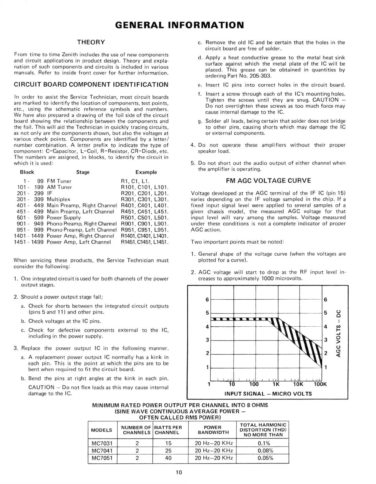
FM AGC VOLTAGE CURVE
Voltage developed at the AGC terminal of the IF IC (pin 15)
varies depending on the IF voltage sampled in the chip. If a
fixed input signal level were applied to several samples of a
given chassis model, the measured AGC voltage for that
input level will vary among the samples. Voltage measured
under these conditions is not a complete indicator of proper
AGC action.
Two important points must be noted:
1.
General shape of the voltage curve (when the voltages are
When servicing these products, the Service Technician must plotted for a curve).
consider the following:
2.
AGC voltage will start to drop as the RF input level in-
1.
One integrated circuit is used for both channels of the power creases to approximately 1000 microvolts.
output stages. • • • • • • •
2.
Should a power output stage
fail;
a. Check for shorts between the integrated circuit outputs
(pins 5 and 11) and other pins.
b. Check voltages at the IC pins.
c. Check for defective components external to the IC,
including in the power supply.
3. Replace the power output IC in the following manner.
a. A replacement power output IC normally has a kink in
each pin. This is the point at which the pins are to be
bent when required to fit the circuit board.
b. Bend the pins at right angles at the kink in each pin.
CAUTION — Do not flex leads as this may cause internal
damage to the IC.
MINIMUM RATED POWER OUTPUT PER CHANNEL INTO 8 OHMS
(SINE WAVE CONTINUOUS AVERAGE POWER -
OFTEN CALLED RMS POWER)
MODELS
NUMBER OF
CHANNELS
WATTS PER
CHANNEL
POWER
BANDWIDTH
TOTAL HARMONIC
DISTORTION (THD)
NO MORE THAN
MC7031
2 15
20 Hz-20 KHz
0.1%
MC7041 2 25
20 Hz-20 KHz 0.08%
MC7051 2
40
20 Hz-20 KHz 0.05%
10
 Loading...