MC96FM204/FM214
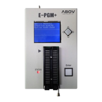
Figure 1.2 PGMplusUSB (Single Writer) ................................................................................................. 13
Figure 1.3 StandAlone PGMplus (Single Writer) ..................................................................................... 13
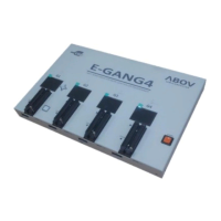
Figure 1.4 StandAlone Gang8 (for Mass Production) ............................................................................. 13
Figure 2.1 Block Diagram ....................................................................................................................... 14
Figure 3.1 MC96FM204 20SOP/TSSOP Pin Assignment....................................................................... 15
Figure 3.2 MC96FM204 16SOP/TSSOP Pin Assignment....................................................................... 16
Figure 3.3 MC96FM214 16SOP/TSSOP Pin Assignment....................................................................... 16
Figure 4.1 20-Pin SOP Package ............................................................................................................. 17
Figure 4.2 20-Pin TSSOP Package ........................................................................................................ 18
Figure 4.3 16-Pin SOP Package ............................................................................................................. 19
Figure 4.4 16-Pin TSSOP Package ........................................................................................................ 20
Figure 6.1 General Purpose I/O Port ...................................................................................................... 23
Figure 6.2 External Interrupt I/O Port ...................................................................................................... 24
Figure 7.1 AC Timing .............................................................................................................................. 31
Figure 7.2 SPI Timing ............................................................................................................................. 32
Figure 7.3 Stop Mode Release Timing when Initiated by an Interrupt .................................................... 33
Figure 7.4 Stop Mode Release Timing when Initiated by RESETB ........................................................ 33
Figure 7.5 Crystal/Ceramic Oscillator ..................................................................................................... 35
Figure 7.6 External Clock ........................................................................................................................ 35
Figure 7.7 Clock Timing Measurement at XIN ........................................................................................ 36
Figure 7.8 Operating Voltage Range ...................................................................................................... 36
Figure 7.9 Recommended Circuit and Layout ......................................................................................... 37
Figure 7.10 Recommended Circuit and Layout with SMPS Power ......................................................... 38
Figure 7.11 RUN (IDD1, XIN=8MHz) Current ......................................................................................... 39
Figure 7.12 RUN (IDD1, HFIRC=8MHz) Current .................................................................................... 39
Figure 7.13 RUN (IDD1, LFIRC=250kHz) Current .................................................................................. 40
Figure 7.14 IDLE (IDD2, XIN=8MHz) Current ......................................................................................... 40
Figure 7.15 IDLE (IDD2, HFIRC =8MHz) Current ................................................................................... 41
Figure 7.16 IDLE (IDD2, LFIRC=250kHz) Current .................................................................................. 41
Figure 7.17 STOP (IDD5, XIN=8MHz) Current ....................................................................................... 42
Figure 8.1 Program Memory ................................................................................................................... 44
Figure 8.2 Data Memory Map ................................................................................................................. 45
Figure 8.3 Lower 128 Bytes RAM ........................................................................................................... 46
Figure 10.1 External Interrupt Description .............................................................................................. 65
Figure 10.2 Block Diagram of Interrupt ................................................................................................... 66
Figure 10.3 Interrupt Vector Address Table ............................................................................................ 68
Figure 10.4 Effective Timing of Interrupt Enable Register...................................................................... 69
Figure 10.5 Effective Timing of Interrupt Flag Register ........................................................................... 69
Figure 10.6 Effective Timing of Interrupt ................................................................................................. 70
Figure 10.7 Interrupt Response Timing Diagram .................................................................................... 71
Figure 10.8 Correspondence between Vector Table Address and the Entry Address of ISP ................. 71
Figure 10.9 Saving/Restore Process Diagram and Sample Source ....................................................... 71
Figure 10.10 Timing Chart of Interrupt Acceptance and Interrupt Return Instruction .............................. 72
Figure 11.1 Clock Generator Block Diagram .......................................................................................... 79
Figure 11.2 Basic Interval Timer Block Diagram ..................................................................................... 82
Figure 11.3 Watch Dog Timer Interrupt Timing Waveform...................................................................... 84
Figure 11.4 Watch Dog Timer Block Diagram ......................................................................................... 85
Figure 11.5 8-Bit Timer/Counter Mode for Timer 0 ................................................................................. 87


 To Next Page