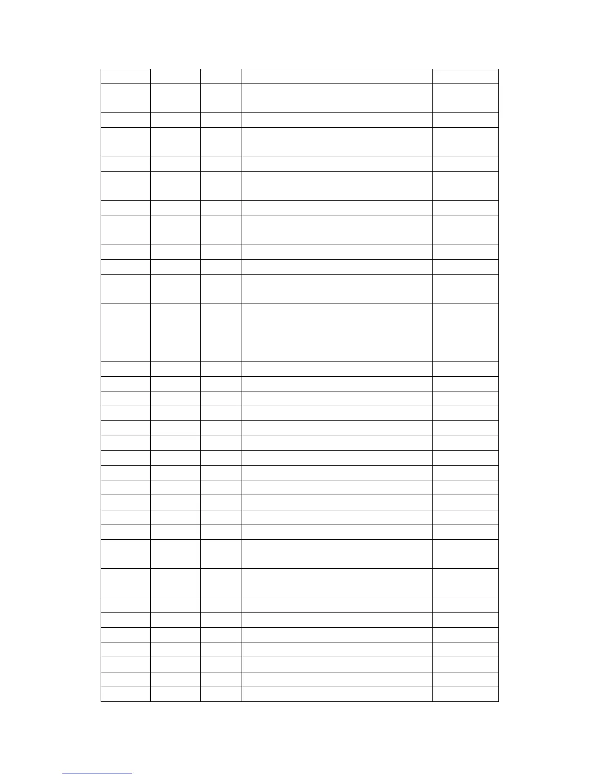
12 VSS Gnd Core Power return 0
13 FIELD Out Odd/Even Field or multi-purpose Output
pin
1.75
14
AMCLK
Out Field locked audio clock output 1.34
15
AMXCL
K
In Audio clock input 0.06
16 ASCLK Out Audio bit serial clock 0.06
17 ALRCL
K
Out Audio frame clock 0.06
18 VSS Gnd Core Power return 0
19 TMODE In This pin is used to enable the in-circuit
test mode
0
20-29 NC 0
30 AVS Gnd Analog 2.5V Power return 0
31 VIN0 In The analog V input to the V-ADC in
component video input mode
2.49
32 VIN1/M
UX4
In This is software selectable input pin for
eigher analog V input to the V-ADC in
component video input mode or analog
composite video input MUX4 to Y-ADC
0.40
33 AVD PI +2.5V Power supply for analog circuity 2.53
34 YBOUT Out Buffered analog output 0.99
35 MUX3 In Analog CVBS or Y input 0.35
36 MUX2 In Analog CVBS or Y input 0.30
37 MUX1 In Analog CVBS or Y input 0.04
38 MUX0 In Analog CVBS or Y input 0.14
39 YGND Gnd Signal ground for Y-ADC 0
40 AVS Gnd Analog 2.5V Power return 0
41 CGND Gnd Signal ground for C-ADC 0
42 CIN0 In Analog chroma input 1.31
43 CIN1 In Analog chroma input 1.59
44 AVD PI +2.5V Power supply for analog circuity 2.53
45 AVSPL
L
Gnd Analog +3.3V Power return 0
46 AVDPL
L
PI Analog +3.3V Power supply 3.43
47 PDN In Power down control pin 0.06
48 SIAD0 In The MPU interface address select pin 0 0.06
49 SCLK In The MPU Serial interface Clock Line 4.00
50 SDAT I/O The MPU Serial interface Data Line 4.00
51 RST# In Master Reset Input 3.41
52 VSS Gnd Core Power return 0
53 VDD PI +2.5V power supply for digital circuitry 2.52
ˋ