Pin Function Type Description
27 D9/PWM Digital GPIO; can be used as PWM
28 D10/PWM Digital GPIO; can be used as PWM
29 D11/MOSI Digital SPI MOSI; can be used as GPIO
30 D12/MISO Digital SPI MISO; can be used as GPIO
5.3 Debug
On the bottom side of the board, under the communication module, debug signals are arranged as 3x2 test pads
with 100 mil pitch. Pin 1 is depicted in Figure 3 – Connector Positions
Pin Function Type Description
1 +3V3 Power Out Internally generated power output to be used as voltage reference
2 SWD Digital SAMD11 Single Wire Debug Data
3 SWCLK Digital In SAMD11 Single Wire Debug Clock
4 UPDI Digital ATMega4809 update interface
5 GND Power Power Ground
6 RST Digital In Active low reset input
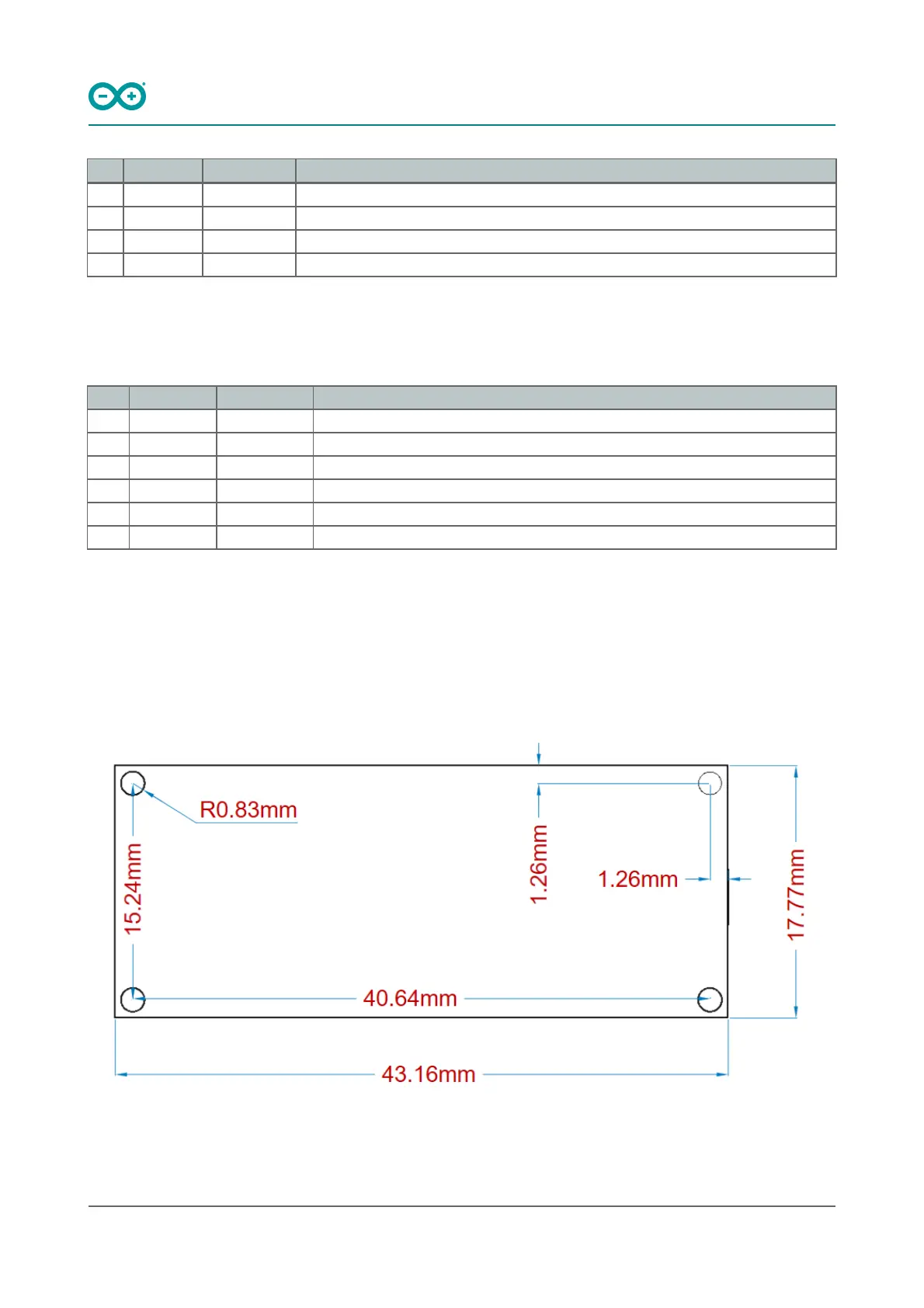
6 Mechanical Information
6.1 Board Outline and Mounting Holes
The board measures are mixed between metric and imperial. Imperial measures are used to maintain a 100 mil
pitch grid between pin rows to allow them to fit a breadboard whereas board length is Metric.
Layout
 Loading...