EasyManuals Logo

Arduino Nano 33 BLE User Manual

Arduino Nano 33 BLE
15 pages
To Next Page IconTo Next Page
To Previous Page IconTo Previous Page
Page #11 background imageLoading...
Page #11 background image
Arduino® Nano 33 BLE
11 / 15 Arduino® Nano 33 BLE / Rev. 01 - 26/11/2021
4.3 Debug
On the bottom side of the board, under the communication module, debug signals are arranged as 3x2 test pads
with 100 mil pitch with pin 4 removed. Pin 1 is depicted in Figure 3 – Connector Positions
Pin Function Type Description
1 +3V3 Power Out Internally generated power output to be used as voltage reference
2 SWD Digital nRF52480 Single Wire Debug Data
3 SWCLK Digital In nRF52480 Single Wire Debug Clock
5 GND Power Power Ground
6 RST Digital In Active low reset input
1 +3V3 Power Out Internally generated power output to be used as voltage reference
5 Mechanical Information
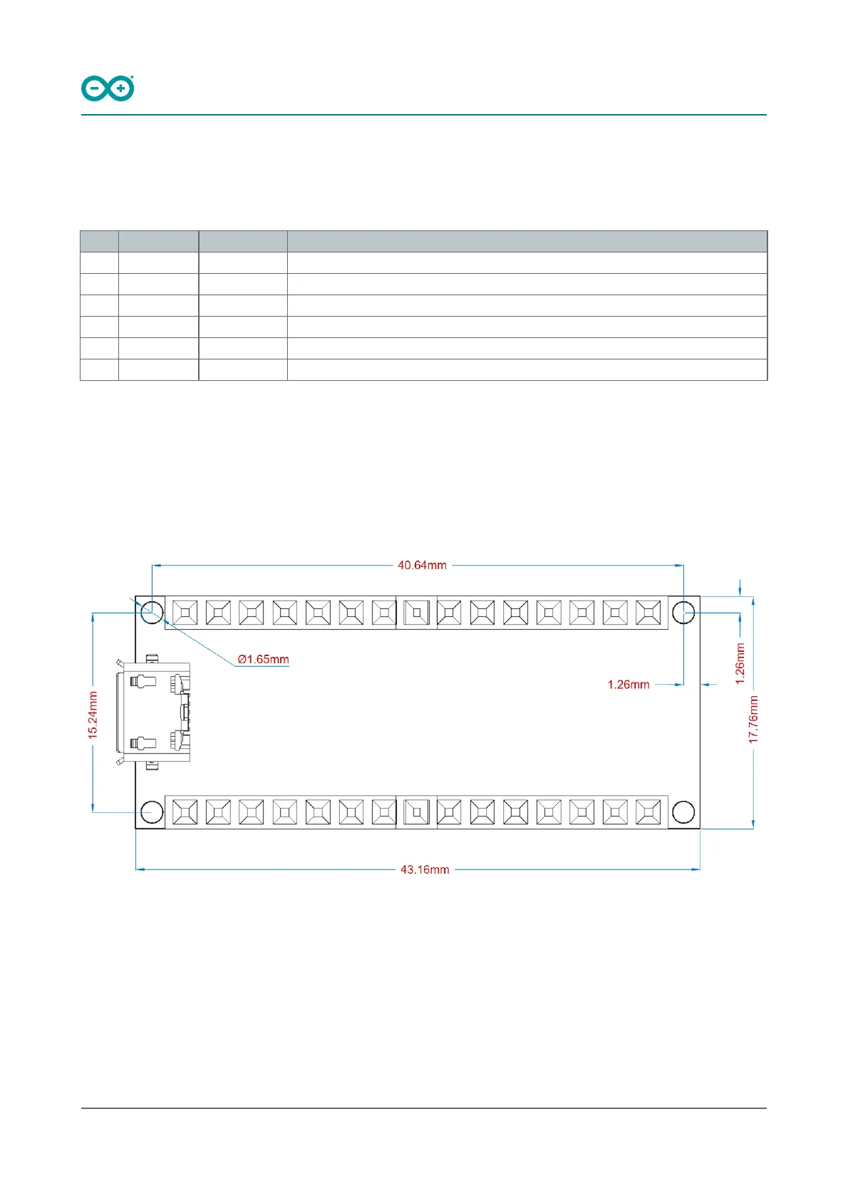
5.1 Board Outline and Mounting Holes
The board measures are mixed between metric and imperial. Imperial measures are used to maintain 100 mil pitch
grid between pin rows to allow them to fit a breadboard whereas board length is Metric
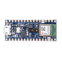
Board layout
Questions and Answers:

Question and Answer IconNeed help?

Do you have a question about the Arduino Nano 33 BLE and is the answer not in the manual?

Arduino Nano 33 BLE Specifications

General IconGeneral
MicrocontrollernRF52840
Operating Voltage3.3V
Input Voltage (limit)21V
Digital I/O Pins14
Analog Input Pins8
DC Current per I/O Pin15 mA
Flash Memory1 MB
SRAM256 KB
Clock Speed64 MHz
BluetoothBluetooth 5.0
External InterruptsAll Digital Pins
Weight5 g
Dimensions45 mm x 18 mm
Analog Output Pins1
USBMicro USB

Related product manuals