the configuration microSD card. The system register interface can implement runtime control of the
OSCs.
PLLs within the FPGA can use the reference 24MHz to generate other fixed internal frequencies.
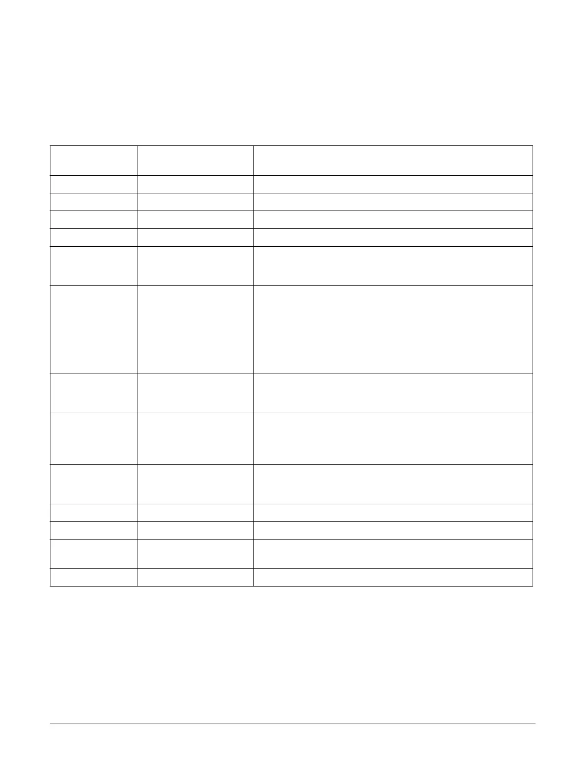
The following table lists the MPS3 board clocks and their characteristics.
Table 2-1 MPS3 board clocks
Clock name:
Source
Programmable frequency
range
Destination: Description
24MHz 24MHz fixed FPGA OSCCLK[0]
OSC1 2-230MHz FPGA OSCCLK[1]
OSC2 2-230MHz FPGA OSCCLK[2]
OSC3 2-230MHz FPGA OSCCLK[3]
OSC3A 12MHz default
USB 2.0 controller.
12MHz is required by USB 2.0 controller.
OSC4 2-230MHz
FPGA OSCCLK[4].
The preferred use for this clock is as the clock for the audio codec and FGPA
audio interface. In this case, this clock is the source clock for:
• AACI_MCLK.
• AACI_SCLK.
• AACI_LRCLK.
OSC0 25MHz default
Ethernet controller.
25MHz required by Ethernet controller.
OSC5 2-230MHz
FPGA OSCCLK[5].
The preferred use for this clock is for the HDMI controller and HDLCD
interface in FPGA.
OSC6 100MHz default
DDR PHY.
100MHz required by DDR PHY.
OSC8MHz 8MHz fixed MCC main input clock.
OSC32K 32.768kHz fixed Input for Real Time Clock (RTC) in MCC.
TCK: JTAG - Source clock for JTAG debug system. Frequency depends on the debugger
setting.
CFGCLK: MCC 25MHz fixed Configuration clock for FPGA.
Related information
1.3 Location of components on the MPS3 board on page 1-15
2 Hardware description
2.3 Clocks
100765_0000_04_en Copyright © 2017–2020 Arm Limited or its affiliates. All rights
reserved.
2-24
Non-Confidential