Last update: 2021/12/20 16:41 ms2000_operation https://asiimaging.com/docs/ms2000_operation
https://asiimaging.com/docs/ Printed on 2022/03/16 04:45
PIN DESCRIPTION FUNCTION FIRMWARE Modules
2 TTL OUT0
TTL OUTPUT – (Usually wire
to the OUT BNC on systems
without PIEZO)
All builds – see TTL command for specific
functions.
3 GND Ground for all I/O
4 TTL IN0 - OUT
OUTPUT – IN0 buffered and
inverted
Can be used as buffered encoder pulses OUTPUT
with ENC_INT.
5 PZ-DAC OUT
ANALOG OUTPUT (0-10v)
from 16 bit DAC
(Wire to OUT BNC on PIEZO
(PZ) systems)
On systems with a PIEZO axis this is the controled
voltage when a commanded move to the PIEZO
(usually Z) axis is made.
DAC_OUT with WRDAC command, provides
external analog output.
6 TTL IN1 INPUT – Auxiliary TTL input
7 SCAN SYNC
OUTPUT for SCAN MODULE
SYNC pulse
SCAN MODULE - selects sync source from JP1 to
clock the sync flip-flop.
Internal Jumper JP1 selects the encoder flag signal that is used for the SYNC flip-flop. JP1 1-2 selects
the X-axis; JP1 2-3 selects the Y-axis.
Internal Jumper JP2 selects the encoder signals that are counted during scanning. JP2 1-2 selects the
X-axis; JP2 2-3 selects the Y-axis.
Please contact ASI if you need assistance configuring the controller for special functions.
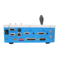
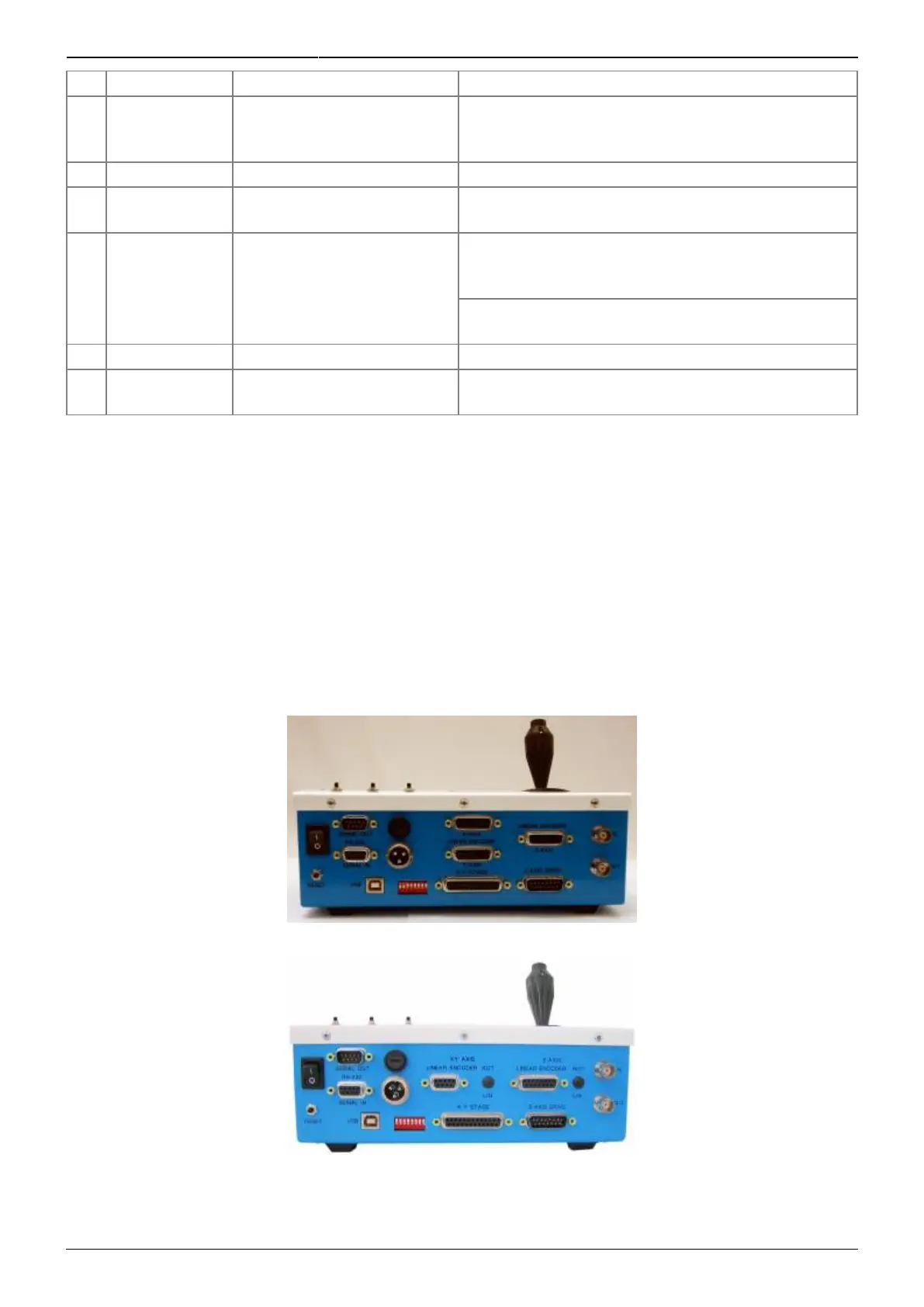
Back Panel Connector Pin-outs