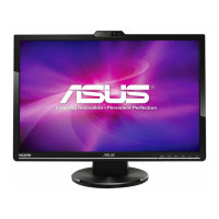
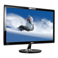
Service Manual ASUS VK266H&VW266H
2
Index
Revision Lists…............................................................................................................................ 3
Important Safety Notice…………………………………………………………………………………..4
1. Monitor Specification..............................……….........................................................................5
2. Operation Instruction…………………………………………………………………………………..6
2.1. General Instructions...........................…............................................................................ 6
2.2.Control Button…………….…..............……......................................................................... 6
2.3.OSD Menu…………….…...........................…......................................................................8
3. Input/Output Specification............……………..........................................................................12
3.1. Input Signal Connector............…………...........................................................................12
3.2. Power Supply Requirements............................................................................................ 13
3.3. Factory Preset Display Modes…….................................................................................. 14
4. Block Diagram…..….....................………….............................................................................17
4.1Software Flow Chat................................................................................................................17
4.2.Electrical Block Diagram........................................................................................................19
5. Schematic Diagram……………………....…............................................................................ 21
5.1. Main Board……….............................................................................................................21
5.2. Power Board...…….......................................................................................................... 31
5.3. USB Board...……....................................................................................................... ….33
5.4. Key Board…………….......................................................................................................34
6. PCB Layout...………................................................................................................................35
6.1. Main Board……….............................................................................................................35
6.2. Power Board…................................................................................................................. 38
6.3. USB Board…...................................................................................................................41
6.4. Key Board……………................................... ...................................................................41
7. Disassemble & Assemble SOP.……………….. ............................................................... …..42
8. ISP Instruction………..............................................................................................................59
9. DDC Instruction…………………………........... .......................................................................68
10. Color/White Balance Adjustment……………........................................................................ 90
11. Trouble Shooting……………………….................................................................................. 92
12. Exploded View…..……………………..... ......................................................................... .....98
13. BOM List………………………………….............................................................................. 100
14. Different Parts List...............................................................................................................146

 Loading...