Microcontroller
5-112
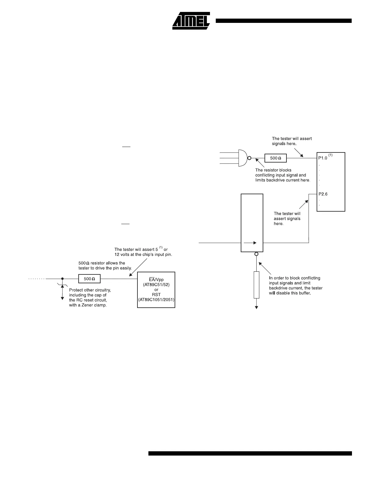
that this pin be “strapped” to V
CC
or ground. Please
interpret the word “Strapped” to mean “connected
by a 500 Ω resistor.” The resistor will supply the
desired 0 or 1 logic level during normal board oper-
ation, but the tester can also change the level easily
as needed when testing the microcontroller or when
writing its flash memory.
2. The pin must be accessible to the tester, i.e. it must
be contactable by a probe in a vacuum fixture (bed-
of-nails fixture).
3. Atmel makes two versions of the microcontroller.
One writes flash memory with 5 volts on this pin; the
other writes flash memory with 12 volts on this pin.
If you are using the 12-volt part, and if you need to
connect other components to the EA
/V
PP
pin for any
reason, you will need to provide some way of pro-
tecting the other components from being damaged
by the 12-volt level. The AT89C1051/2051 are only
available with 12-volt programming.
4. For the AT89C1051/2051, if an RC circuit is used to
generate power-up reset, don’t tie the capacitor
directly to the RST pin. Put a resistor in between so
that the tester will not have to take time charging the
capacitor to 12 volts with each programmed byte.
Figure 1.
Allow the tester to control EA
/V
PP
/RST, and pro-
tect surrounding devices.
Note: 1. Only for the AT89C51 or AT89C52
Data Ports (P0, P1, P2, P3 for AT89C51/52 and
P1, P3 for AT89C1051/2051)
The normal mission of the board may set these ports up to
be outputs, or inputs, or a mix of outputs and inputs. During
flash memory write and erase operations, the tester will
apply signals to some of these pins, and attempt to read
signals from others. Outputs of other circuits on the board
may be exposed to excessive backdrive, or may interfere
with output signals trying to come from the microcontroller.
There are three things to remember about these pins.
1. The pins must be accessible to the tester, i.e. it
must be contactable by probes in a vacuum fixture.
2. If any other chips have their outputs connected to
pins used as inputs, they must be protected from
backdrive signals coming from the tester. Pass such
signals through disableable buffers as shown in Fig-
ure 2 below. Alternatively you may insert a 500 Ω
resistor in series with such an output as also shown
in Figure 2 below. The resistor will limit the back-
drive current to 5 volts/500 ohms = 10 milliamps.
The port pins used as inputs are all of P0, all of P1,
P2.0-P2.4, P2.6, P2.7, P3.6, and P3.7 for the
AT89C51/52 and P1 for the AT89C1051/2051.
Figure 2.
Allow the tester to assert signals safely on micro-
controller pins that serve as inputs during flash memory
writing and erasing.
Note: 1. For the AT89C1051/2051 the tester disable P1 input
signals originating on the board during flash mem-
ory writing and erasing.
3. If any other chips have their outputs connected to
pins used as outputs during flash memory writing
and erasing operations, pass such signals through
disableable buffers as shown in Figure 3. Attempt-
ing to isolate with a 500 Ω resistor will not work,
due to the small amount of output current available
from the device. A 10K pullup is required to ensure
an adequate high for the tester to measure. The
port pins used as inputs are all of P0 and P3.4 for
the AT89C51/52 and P1 for the AT89C1051/2051.

 Loading...