Microcontroller
5-113
Figure 3.
Be sure spurious signals do not conflict with
AT89C51/52 pins used as outputs during flash writing and
erasing.
Note on Lock Bits
Do not program the DFP to set any of the Lock Bits until
you are certain the other parts of the flash writing program
have been fully debugged.
DFP Wiring
One possible way of wiring the DFP to write the devices is
described in the tables. Two DR2p cards (that is, one from
the base unit and one expansion kit) are required for one
AT89C51/52 chip, and one DR2p card is required for each
AT89C1051/2051 chip on the board.
Using the Atmel AT89C51 or AT89C52
RST
The tester will take this pin high during flash memory write
and erase operations. It will be low when the board is carry-
ing out its normal mission, unless frequent resetting is an
integral part of the board’s normal mission. There are three
things to remember about this pin.
1. Most AT89C52 circuits have a simple RC reset cir-
cuit in which a large capacitor is wired between the
RST pin and ground. When the tester drives the
RST pin high to initiate an erasure or writing of the
flash memory, several microseconds may be
required to allow the tester's channel driver to
charge the capacitor.
2. The pin must be accessible to the tester, i.e. it must
be contactable by probe in a vacuum fixture.
3. Because the tester will force the pin high, you must
design other circuitry on this pin to permit and toler-
ate the forced high.
PSEN
The tester takes this pin low during flash memory write and
erase operations. Other than that, it is not supposed to be
connected to anything else. There is one thing to remem-
ber about this pin.
1. The pin must be accessible to the tester, i.e. it must
be contactable by probe in a vacuum fixture.
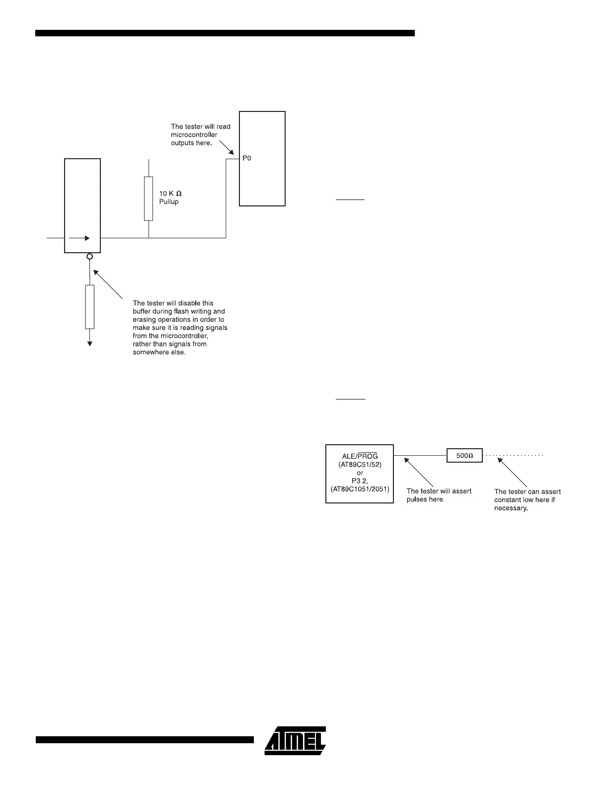
ALE/PROG
This pin is normally an output from the chip, but the tester
will use it as a command strobe input during flash memory
write and erase operations. There are three things to
remember about this pin.
1. The pin must be accessible to the tester, i.e. it must
be contactable by a probe in a vacuum fixture.
2. If any other chips have their outputs connected to
this pin (unlikely, but please check) they must be
capable of being disabled by the tester. Alternatively
you may design a 500 Ω resistor in series with such
an output. The resistor will protect the other chip
from excessive backdrive, and will also prevent the
other chip from volunteering spurious strobes dur-
ing the flash memory writing or erasing processes.
Figure 4.
500 Ω resistor allows the tester to drive the
ALE/PROG
for AT89C51/52 or P3.2 (AT89C1051/2051)
pin easily and keeps downstream circuits from seeing
unusual activity.
3. Flash memory writing and erasing cycles generate
activity in other parts of the circuit. If any other chips
or subsystems on the board are designed to
respond to the ALE signal, they will receive unusual
instructions during the writing and erasing cycles.
Be sure that this unusual activity does not damage
them. Things to look for are other in-circuit writable
nonvolatile devices, fusible squibs, etc. If any such
exist, the 500 Ω resistor method described above
for disabling outputs will also the tester to prevent
the sensitive subsystems from seeing the unusual
ALE activity.

 Loading...