t
XHDV
t
QVXH
t
XLXL
t
XHDX
t
XHQX
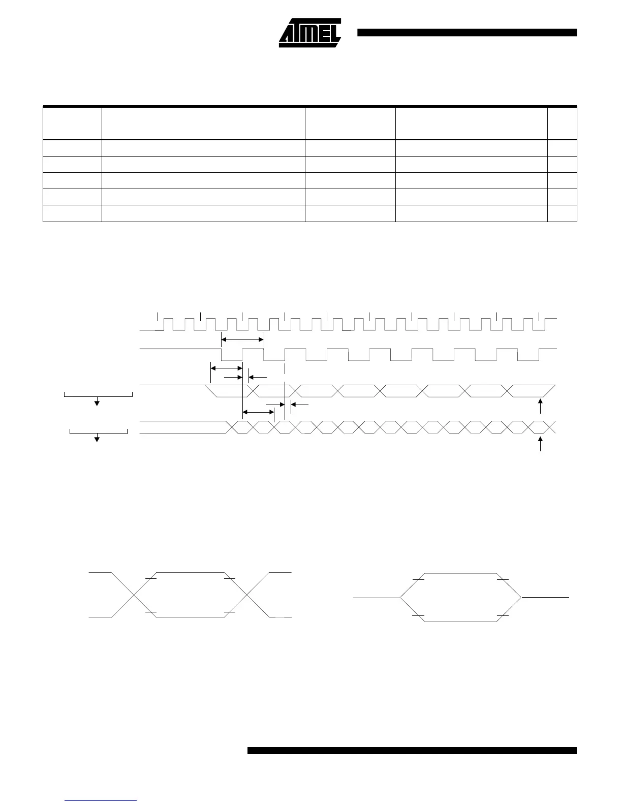
ALE
INPUT DATA
CLEAR RI
OUTPUT DATA
WRITE TO SBUF
INSTRUCTION
CLOCK
0
0
1
1
2
2
3
3
4
4
5
5
6
6
7
7
SET TI
SET RI
8
VALID VALIDVALID VALIDVALID VALIDVALID VALID
Shift Register Mode Timing Waveforms
0.45V
TEST POINTS
V - 0.5V
CC
0.2 V + 0.9V
CC
0.2 V - 0.1V
CC
AC Testing Input/Output Waveforms
(1)
Note: 1. AC Inputs during testing are driven at V
CC
- 0.5 V
for a logic 1 and 0.45 V for a logic 0. Timing meas-
urements are made at V
IH
min. for a logic 1 and
V
IL
max. for a logic 0.
Serial Port Timing: Shift Register Mode Test Conditions
The values in this table are valid for V
CC
= 5.0 V ± 20% and Load Capacitance = 80 pF.
Symbol Parameter
12 MHz Osc Variable Oscillator
Units
Min Max Min Max
t
XLXL
Serial Port Clock Cycle Time 1.0 12t
CLCL
µs
t
QVXH
Output Data Setup to Clock Rising Edge 700 10t
CLCL
-133 ns
t
XHQX
Output Data Hold After Clock Rising Edge 50 2t
CLCL
-33 ns
t
XHDX
Input Data Hold After Clock Rising Edge 0 0 ns
t
XHDV
Clock Rising Edge to Input Data Valid 700 10t
CLCL
-133 ns
V
LOAD
+ 0.1V
Timing Reference
Points
V
LOAD
- 0.1V
LOAD
V
V
OL
+ 0.1V
V
OL
- 0.1V
Float Waveforms
(1)
Note: 1. For timing purposes, a port pin is no longer floating
when a 100-mV change from load voltage occurs. A
port pin begins to float when a 100-mV change from
the loaded V
OH
/V
OL
level occurs.
20 AT89C52
 Loading...


