EasyManua.ls Logo

Atmel AT89C52 User Manual

Atmel AT89C52
22 pages
To Next Page IconTo Next Page
Page #1 background imageLoading...
Page #1 background image
8-Bit
Microcontroller
with 8 Kbytes
Flash
AT89C52
Features
Compatible with MCS-51
TM
Products
8 Kbytes of In-System Reprogrammable Flash Memory
Endurance: 1,000 Write/Erase Cycles
Fully Static Operation: 0 Hz to 24 MHz
Three-Level Program Memory Lock
256 x 8-Bit Internal RAM
32 Programmable I/O Lines
Three 16-Bit Timer/Counters
Eight Interrupt Sources
Programmable Serial Channel
Low Power Idle and Power Down Modes
(T2) P1.0
V
CC
(T2 EX) P1.1
P0.0 (AD0)
P1.2
(INT0) P3.2
ALE/PROG
(RD) P3.7 P2.3 (A11)
(TXD) P3.1
EA/VPP
(WR) P3.6
P2.4 (A12)
(RXD) P3.0
P0.7 (AD7)
(T1) P3.5
P2.6 (A14)
RST
P0.6 (AD6)
P0.5 (AD5)
P0.4 (AD4)
P0.3 (AD3)
P0.2 (AD2)
P1.3
P0.1 (AD1)
(INT1) P3.3
PSEN
XTAL2 P2.2 (A10)
(T0) P3.4
P2.7 (A15)
XTAL1 P2.1 (A9)
GND P2.0 (A8)
P2.5 (A13)
20
19
18
17
16
15
1
2
3
4
5
6
7
8
9
10
11
12
13
14
21
22
23
24
25
26
40
39
38
37
36
35
34
33
32
31
30
29
28
27
(SS) P1.4
(MOSI) P1.5
(MISO) P1.6
(SCK) P1.7
Pin Configurations
PDIP/Cerdip
Description
The AT89C52 is a low-power, high-performance CMOS 8-bit microcomputer with 8
Kbytes of Flash programmable and erasable read only memory (PEROM). The de-
vice is manufactured using Atmel’s high density nonvolatile memory technology and
is compatible with the industry standard 80C51 and 80C52 instruction set and pinout.
The on-chip Flash allows the program memory to be reprogrammed in-system or by
a conventional nonvolatile memory programmer. By combining a versatile 8-bit CPU
with Flash on a monolithic chip, the Atmel AT89C52 is a powerful microcomputer
which provides a highly flexible and cost effective solution to many embedded control
applications.
(continued)
23
1
INDEX
CORNER
34
P1.0 (T2)
VCC
P1.1 (T2 EX)
P1.2
P1.3
NC
42
43
40
41
6
5
4
44
3
2
26
25
28
27
24
18
19
20
21
22
NC
7
8
9
10
11
12
13
14
15
16
17
29
30
39
38
37
36
35
33
32
31
NC
PSEN
XTAL1
GND
XTAL2
GND
P0.0 (AD0)
ALE/PROG
(RD) P3.7
EA/VPP
(WR) P3.6
(RXD) P3.0
P0.7 (AD7)
P2.6 (A14)
P0.6 (AD6)
P0.5 (AD5)
P0.4 (AD4)
P0.3 (AD3)
P0.2 (AD2)
P0.1 (AD1)
(INT0) P3.2
(TXD) P3.1
(T1) P3.5
(INT1) P3.3
(T0) P3.4
P2.7 (A15)
(A11) P2.3
(A12) P2.4
(A10) P2.2
(A9) P2.1
(A8) P2.0
RST
P2.5 (A13)
P1.4
(
SS)
(MOSI) P1.5
(MISO) P1.6
(SCK) P1.7
PQFP/TQFP
P1.0 (T2)
VCC
P1.1 (T2 EX)
P0.0 (AD0)
P1.2
ALE/PROG
(RD) P3.7
XTAL1
EA/VPP
(WR) P3.6
GND
(RXD) P3.0
P0.7 (AD7)
P2.6 (A14)
P0.6 (AD6)
P0.5 (AD5)
P0.4 (AD4)
P0.3 (AD3)
P0.2 (AD2)
P1.3
P0.1 (AD1)
PSEN
XTAL2
(INT0) P3.2
(TXD) P3.1
(T1) P3.5
(INT1) P3.3
(T0) P3.4
P2.7 (A15)
(A11) P2.3
(A12) P2.4
(A10) P2.2
(A9) P2.1
(A8) P2.0
NC
23
1
RST
INDEX
CORNER
NC
NC
P2.5 (A13)
34
NC
42
43
40
41
6
5
444
3
2
26
25
28
27
18
19
20 24
21
22
7
8
9
10
11
12
13
14
15
16
17 29
30
39
38
37
36
35
33
32
31
P1.4 (
SS)
(MOSI) P1.5
(MISO) P1.6
(SCK) P1.7
PLCC/LCC
0313E
Question and Answer IconNeed help?

Do you have a question about the Atmel AT89C52 and is the answer not in the manual?

Atmel AT89C52 Specifications

General IconGeneral
Architecture8-bit
ManufacturerAtmel
Core8051
Program Memory Size8 KB
RAM Size256 Bytes
Number of I/O Pins32
UARTYes
PackagePDIP, PLCC, TQFP
Data Bus Width8-bit
Address Bus Width16-bit
Interrupts6
Operating Voltage4.0V - 5.5V
Clock Speed24 MHz

Summary

Description

Block Diagram

Pin Description

Vcc

Supply voltage for the microcontroller.

GND

Ground connection for the microcontroller.

Port 0

8-bit open-drain bidirectional I/O port with multiple functions.

Port 1

8-bit bidirectional I/O port with internal pullups and special functions.

Port 2

8-bit bidirectional I/O port with internal pullups, used for address bus.

Port 3

8-bit bidirectional I/O port with internal pullups and special function pins.

RST

Reset input pin; high for two machine cycles resets the device.

ALE/PROG

Address Latch Enable/Program Pulse input.

EA/VPP

External Access Enable / Programming Voltage input.

XTAL1

Input for oscillator amplifier and clock circuitry.

XTAL2

Output from the inverting oscillator amplifier.

Special Function Registers

Timer 0 and 1

Timer 2

Capture Mode

Two options selected by EXEN2 for capture or overflow interrupts.

Auto-Reload (Up or Down Counter)

Timer 2 counts up/down, reloads from RCAP2H/RCAP2L.

Baud Rate Generator

Timer 2 configured to generate baud rates for serial communication.

Programmable Clock Out

Using Timer 2 to generate a 50% duty cycle clock output.

UART

Interrupts

IE register

Special Function Register for enabling/disabling interrupts.

Interrupt Sources

Description of external and timer interrupts.

Oscillator Characteristics

Idle Mode

Power Down Mode

Program Memory Lock Bits

Programming the Flash

Data Polling

Indicates end of write cycle by complement of written data on PO.7.

Ready/Busy

P3.4 indicates BUSY or READY status during programming.

Program Verify

Reads back programmed code for verification if lock bits are not set.
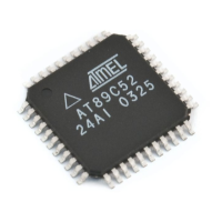
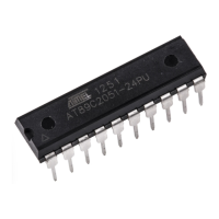
Absolute Maximum Ratings

D.C. Characteristics

A.C. Characteristics

Ordering Information

Related product manuals