60
4929B–AUTO–01/07
ATA6264 [Preliminary]
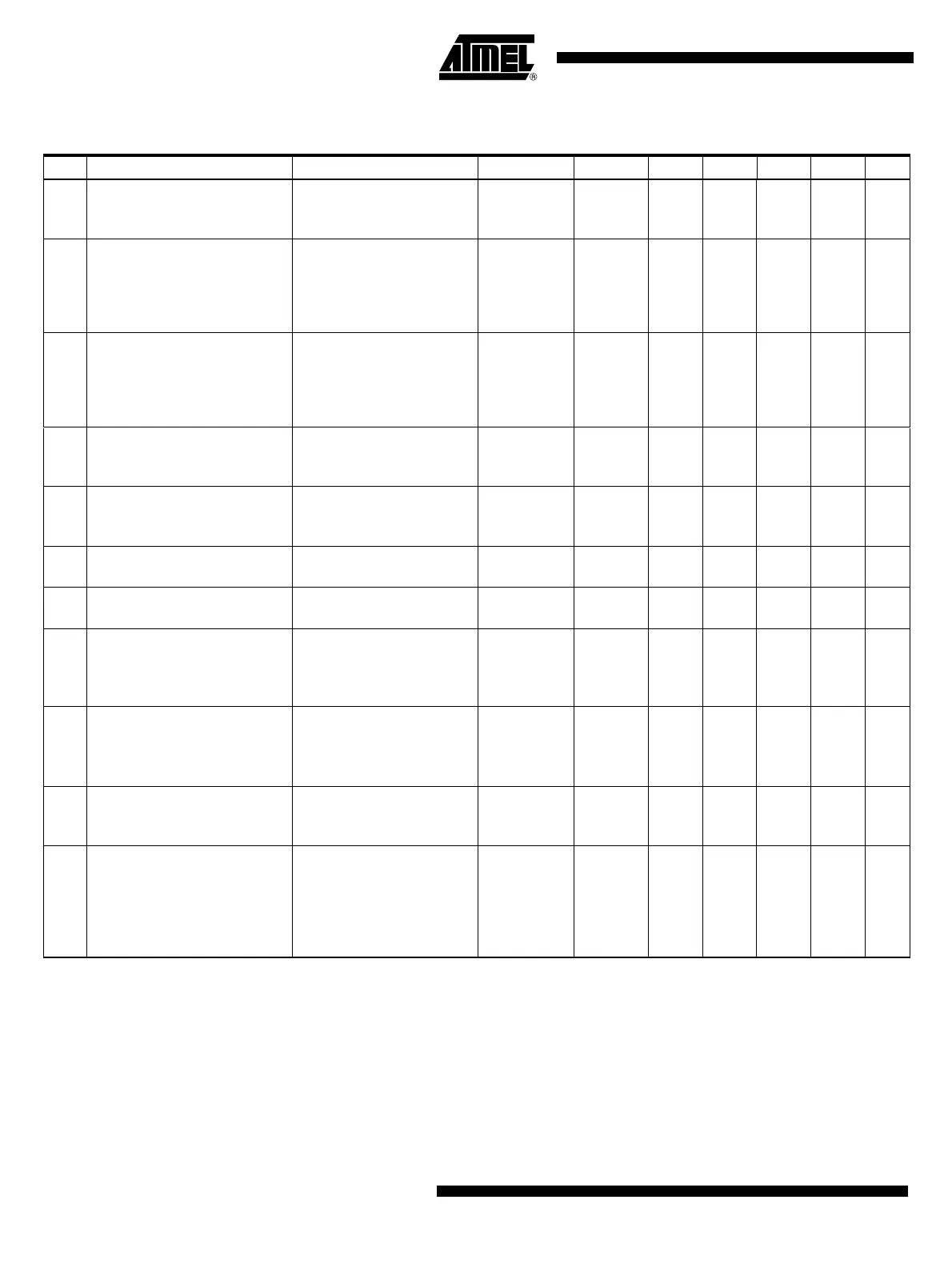
Table 18-1. Electrical Characteristics – Voltage/Current Sources (IASG
x
Sources)
No. Parameters Test Conditions Pin Symbol Min Typ. Max. Unit Type*
17.1 Output voltage (V1)
(x = 1 to 5),
–40 mA < I
IASGx
< –0.5 mA
V
ISENS
= 0.96 × V
VPERI
IASG
x
V1
IASGx
–6% 10 +6% V A
17.2 Output voltage (V2)
(x = 1 to 5),
–40 mA < I
IASGx
< –0.5 mA
V
ISENS
= 0.96 × V
VPERI
IASG
x
switched to 5V
V
EVZ
> 11V
IASG
x
V2
IASGx
–6% 5 +6% V A
17.2a Output voltage (V2)
(x = 1 to 5),
–25 mA < I
IASGx
< –0.5 mA
V
ISENS
= 0.96 × V
VPERI
IASG
x
switched to 5V
V
EVZ
> 9V to 11V
IASG
x
V2
IASGx
–6% 5 +6% V A
17.3
Output voltage overshoot at
IASGx due to regulator
characteristic
(x = 1 to 5)
when IASG = 5V
when IASG = 10V
IASG
x
∆V
IASGx
5.9
11.3
V
V
A
A
17.4
Maximum duration of voltage
overshoot at IASGx
(x = 1 to 5),
with V
IASGx
= 10V / 0.5 mA <
R
LOAD
< V
IASGx
= 5V / 40 mA
IASG
x
t
IASGx
30 µs A
17.5
Linear range for current mirror
at IASGx
(x = 1 to 5),
0V = V
ISENS
= 0.96 × V
PERI
IASG
x
I
IASGx
–40 –0.5 mA A
17.6
Internal current limitation at
IASG
x
(x = 1 to 5) IASG
x
I
IASGx
–150 –50 mA A
17.7 Current ratio #1
(x = 1 to 5),
CR
1x
= I
IASGx
/ I
ISENS
0V = V
ISENS
= 0.96 × V
VPERI
–40 mA < I
IASGx
< –0.5mA
IASG
x
CR
1x
–3% 9.9 +3% A
17.8 Current ratio #2
(x = 1 to 5),
CR
2x
= I
IASGx
/I
ISENS
0V = V
ISENS
= 0.96 × V
VPERI
–40 mA < I
IASGx
< –0.5 mA
IASG
x
CR
2x
–3% 14.9 +3% A
17.9 Settling time
(x = 1 to 5),
R
IASGx
= 250Ω, no capacitive
load at IASGx
ISENSE t
ISENSE
050µsA
17.10 Switch-on delay
(x = 1 to 5)
Measured from rising edge
of SSQ to
V
IASGx
= 0.1 × V
IASGx
R
IASGx
= 250Ω, no
capacitive load at IASGx
IASG
x
t
IASGx
050µsA
*) Type means: A = 100% tested, B = 100% correlation tested, C = Characterized on samples, D = Design parameter
 Loading...