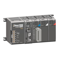
DL06 Micro PLC User Manual, 3rd Edition, Rev. E
iv
Table of Contents
Normal Minimum I/O Response ............................................................................. 3–18
Normal Maximum I/O Response ............................................................................3–18
Improving Response Time ......................................................................................3–19
CPU Scan Time Considerations ...............................................................................3–20
Reading Inputs .......................................................................................................3–20
Writing Outputs .....................................................................................................3–20
Service Peripherals ..................................................................................................3–21
CPU Bus Communication .......................................................................................3–21
Update Clock/Calendar, Special Relays, Special Registers .......................................3–21
Application Program Execution ..............................................................................3–22
PLC Numbering Systems ........................................................................................3–23
PLC Resources ........................................................................................................3–23
V–Memory .............................................................................................................3–24
Binary-Coded Decimal Numbers ............................................................................3–24
Hexadecimal Numbers ...........................................................................................3–24
Memory Map ...........................................................................................................3–25
Octal Numbering System .......................................................................................3–25
Discrete and Word Locations ..................................................................................3–25
V-memory Locations for Discrete Memory Areas ....................................................3–25
Input Points (X Data Type) ..................................................................................... 3–26
Output Points (Y Data Type) ..................................................................................3–26
Control Relays (C Data Type) .................................................................................3–26
Timers and Timer Status Bits (T Data Type) ............................................................3–26
Timer Current Values (V Data Type) .......................................................................3–27
Counters and Counter Status Bits (CT Data type) ...................................................3–27
Counter Current Values (V Data Type) ...................................................................3–27
Word Memory (V Data Type) .................................................................................3–28
Stages (S Data type) ...............................................................................................3–28
Special Relays (SP Data Type) ................................................................................. 3–28
DL06 System V-memory ..........................................................................................3–29
System Parameters and Default Data Locations (V Data Type) ...............................3–29
DL06 Aliases ............................................................................................................. 3–31
DL06 Memory Map ..................................................................................................3–32
X Input/Y Output Bit Map ......................................................................................3–33
Stage Control/Status Bit Map ................................................................................. 3–34
Control Relay Bit Map .............................................................................................3–36
 Loading...