EasyManua.ls Logo

Blaupunkt MVP 01 - Page 7

Blaupunkt MVP 01
63 pages
Print Icon
To Next Page IconTo Next Page
To Previous Page IconTo Previous Page
Loading...
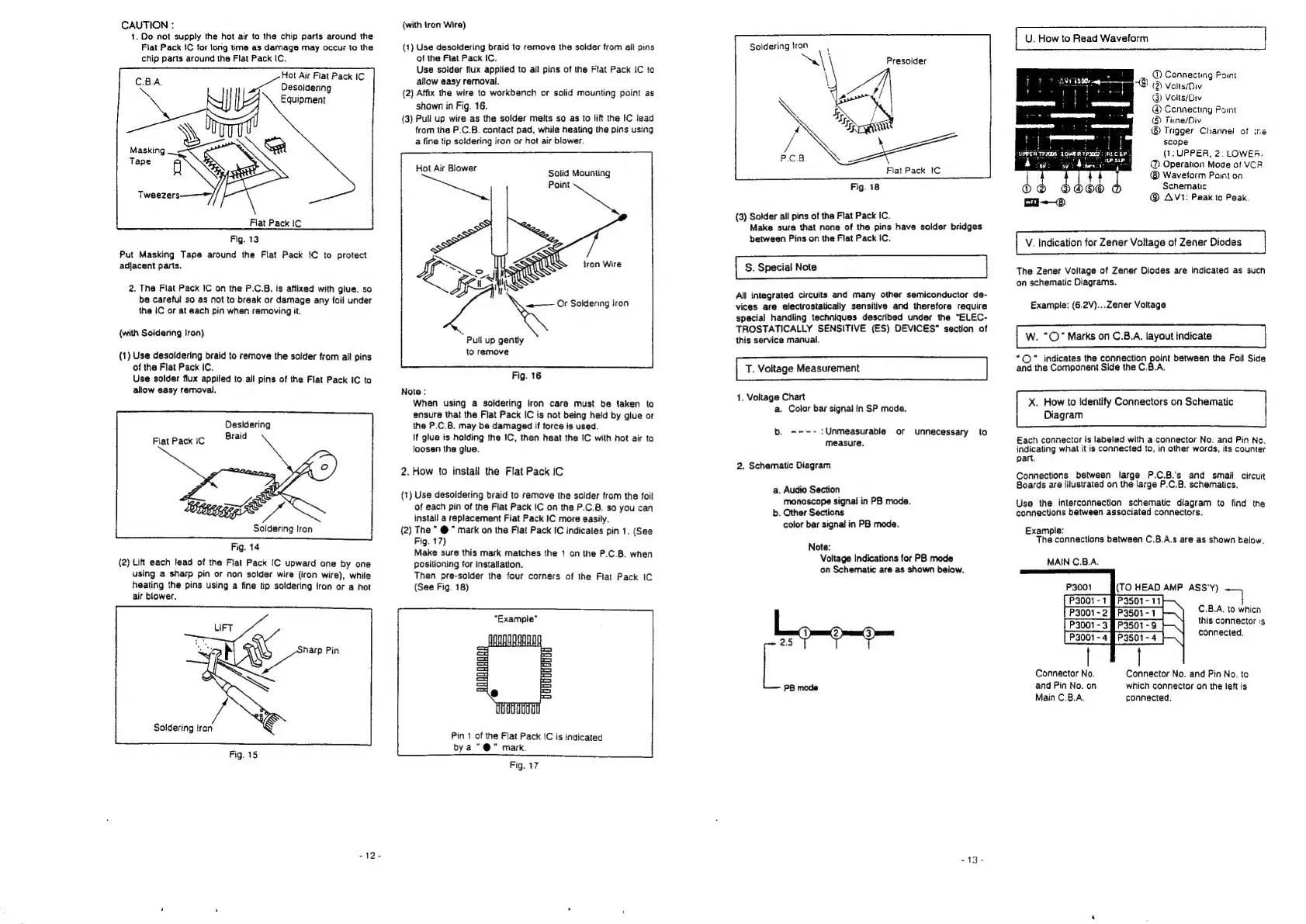
CAUTION
:
1.
Do
not
supply
the
hot
air
to
the
chip
parts
around
the
Fiat
Pack
IC
for
tong
time
as
damage
may
occur
to
the
chip
parts
around
the
Flat
Pack
iC.
Hot
Air
Flat
Pack
IC
C.B.A.
a
Desoldering
og
Equipment
Masking
Sa
Tape
q
Tweezers——"
Flat
Pack
IC
Fig.
13
Put
Masking
Tape
around
the
Flat
Pack
!C
to
protect
adjacent
parts.
2.
The
Flat
Pack
IC
on
the
P.C.B.
is
affixed
with
glue,
so
be
careful
so as
not
to
break
or
damage
any
foil
under
the
iC
or
at
each
pin
when
removing
it.
(with
Soldering
tron)
(1)
Use
desoldering
braid
to
remove
the
soider
from
all
pins
of
the
Flat
Pack
IC.
Use
solder
flux
applied
to
all
pins
of
the
Flat
Pack
IC
to
allow
easy
removal.
Desidering
FlatPackic
Braid
Soldering
Iron
Fig.
14
(2)
Lift
each
lead
of
the
Flat
Pack
IC
upward
one
by
one
using
a
sharp
pin
or
non
solder
wire
(iron
wire),
while
heating
the
pins
using
a
fine
tip
soldering
iron
or
a
hot
air
blower.
Soldering
tron
Fig.
15
{with
tron
Wire)
(1)
Use
desoidering
braid
to
remove
the
solider
trom
ait
pins
of
the
Flat
Pack
IC.
Use
solder
flux
applied
to
al!
pins
of
the
Flat
Pack
IC
to
allow
easy
removal.
{2)
Affix
the
wire
to
workbench
or
solid
mounting
point
as
shown
in
Fig.
16.
{3)
Pull
up
wire
as
the
solder
melts
so
as
to
lift
the
IC
lead
from
the
P.C.B.
contact
pad,
while
heating
the
pins
using
a
fine
tip
soldering
iron
or
hot
air
blower.
Hot
Air
Blower
Solid
Mounting
Point
Se
tron
Wire
~——
Of
Soldering
Iron
Pull
up
gently
to
remove
Fig.
16
Note:
When
using
a
soldering
iron
care
must
be
taken
to
ensure
that
the
Flat
Pack
IC
is
not
being
held
by
giue
or
the
P.C.B.
may
be
damaged
if
force
is
used.
If
glue
is
holding
the
IC,
then
heat
the
IC
with
hot
air
to
loosen
the
glue.
2.
How
to
install
the
Flat
Pack
IC
(1)
Use
desoldering
braid
to
remove
the
solder
from
the
foil
of
each
pin
of
the
Flat
Pack
IC
on
the
P.C.B.
so
you
can
install
a
replacement
Fiat
Pack
IC
more
easily.
(2)
The
”
@
"
mark
on
the
Flat
Pack
IC
indicates
pin
1.
(See
Fig.
17)
Make
sure
this
mark
matches
the
1
on
the
P.C.8.
when
positioning
for
installation.
Then
pre-soider
the
four
corners
of
the
Fiat
Pack
IC
(See
Fig.
18)
“Example”
Pin
1
of
the
Flat
Pack
IC
is
indicated
bya
"@"
mark.
Fig.
17
Soldering
tron
Presoider
Fiat
Pack
IC
Fig.
18
(3)
Solder
all
pins
of
the
Flat
Pack
IC.
Make
sure
that
none
of
the
pins
have
solder
bridges
between
Pins
on
the
Flat
Pack
IC.
S.
Special
Note
All
integrated
circuits
and
many
other
semiconductor
de-
vices
are
electrostatically
sensitive
and
therefore
require
special
handling
techniques
described
under
the
“ELEC-
TROSTATICALLY
SENSITIVE
(ES)
DEVICES”
section
of
this
service
manual.
T.
Voltage
Measurement
1.
Voltage
Chart
a.
Color
bar
signal
in
SP
mode.
b.
----:Unmeasurable
or
unnecessary
to
measure,
2.
Schematic
Diagram
a.
Audio
Section
monoscope
signal
in
PB
mode.
b.
Other
Sections
color
bar
signal
in
PB
mode.
Note:
Voltage
Indications
for
PB
mode
on
Schematic
are
as
shown
below.
2.5
PB
mode
-13-
U.
How
to
Read
Waveform
=,
©
Connecting
Font
“~@
D
vons/Niv
@
Volis/Ow
@
Connecting
Paint
©
Tine/Div
@
Trigger
Channel
of
ine
scope
(1:
UPPER,
2:
LOWER,
@
Operation
Moge
of
VCR
@
Wavetorm
Paint
on
Schematic
m—®
@
AV}:
Peak
to
Peak.
V.
Indication
for
Zener
Voltage
of
Zener
Diodes
The
Zener
Voltage
of
Zener
Diodes
are
indicated
as
such
on
schematic
Diagrams.
Example:
(6.2V)...Zener
Voltage
W.
“©”
Marks
on
C.B.A.
layout
indicate
“©”
indicates
the
connection
gaint
between
the
Foil
Side
and
the
Component
Side
the
C.B.A.
X.
How
to
identify
Connectors
on
Schematic
Diagram
Each
connector
is
labeled
with
a
connector
No.
and
Pin
Nc.
indicating
what
it
is
connected
to,
in
other
words,
its
counter
part.
Connections
between
large
P.C.B.’s
and
small
circuit
Boards
are
illustrated
on
the
large
P.C.B.
schematics,
Use
the
interconnaction
schematic
diagram
to
find
the
connections
between
associated
connectors.
Example:
The
connections
between
C.B.A.s
are
as
shown
below.
MAIN
C.B.A.
(TO
HEAD
AMP
ASS'Y)
(P3001-1
P3501
11]
|
P3001-2§P3s01-1
|
C.B.A.
to
which
[
P3007
-
3]
1Pa501-9
|
this
connector
is
P3001-4
1P3501-4
|
connected.
|
F
|
Connector
No.
Connector
No.
and
Pin
No.
to
and
Pin
No.
on
which
connector
on
the
left
is
Main
C.B.A.
connected.

Related product manuals