— 6 —
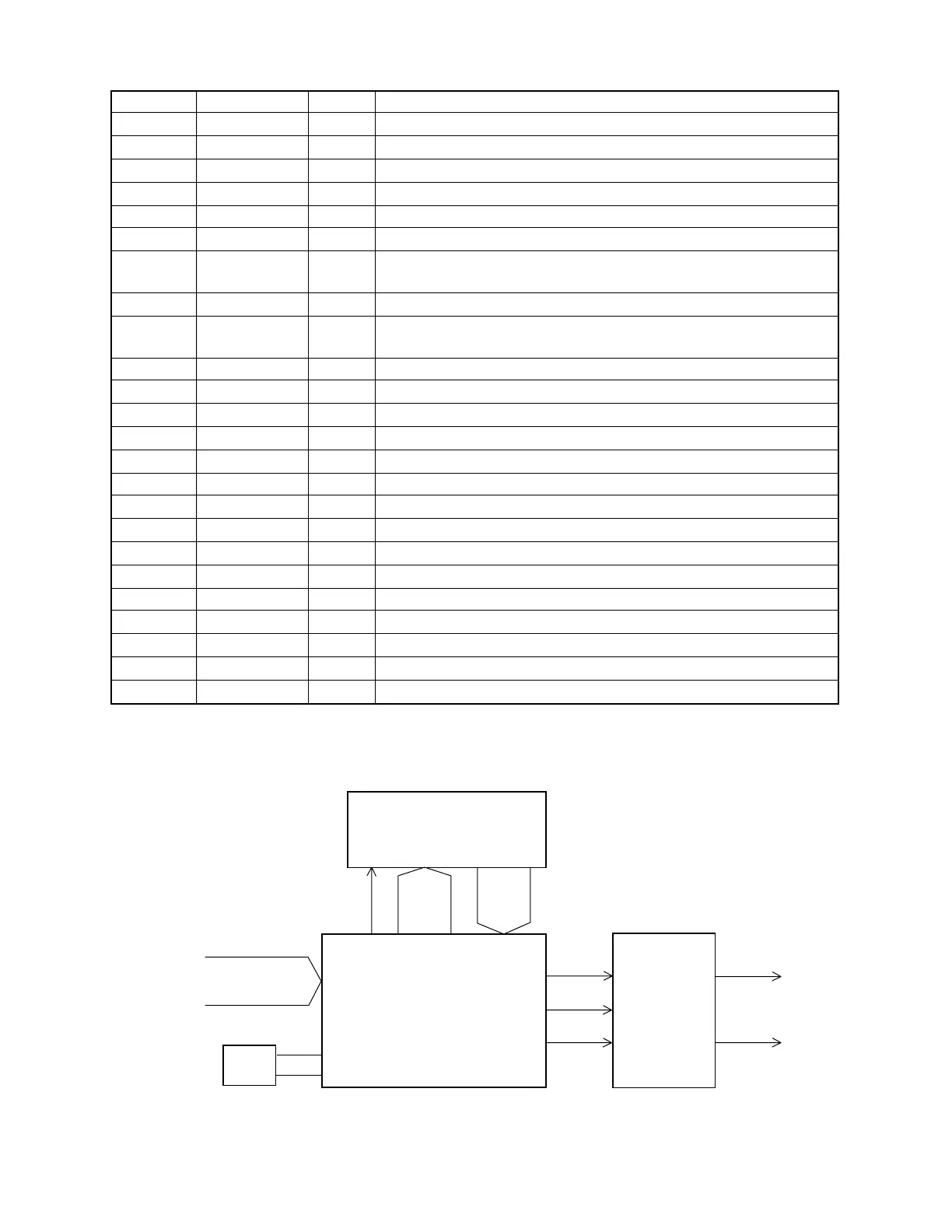
CPU
LSI101
UPD912GF-3BA
Sound Source ROM
LSI102
TC534200CF-C116
CE
A0 ~ A17 D0 ~ D15
MA1 ~
MA18
MD0 ~
MD15
MSB0
FI0 ~ FI9
SI0 ~ SI9
SO
BOK
LRCK
PG
X101
20 MHz
DAC
IC105
UPD6379GR
LOUT
ROUT
SO: Sound data
BOK: Bit clock
LRCK: Word clock
SI
CLK
LRCK
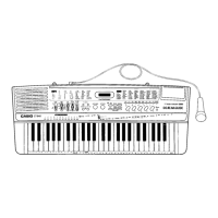
From keyboard
Pin No. Terminal In/Out Function
15, 16 XLT0, XLT1 In/Out 20 MHz clock input/output
17 VCC In +5 V source
18, 19 MD0, MD1 In Mode selection terminal. Connected to ground.
20 RSTB In Reset signal input
21 NMI In Power ON signal input
22 INT — Not used. Connected to ground.
23 ~ 30
FI0 ~ FI3
SI0 ~ SI3
In Key input signal
31 ~ 38 KC0 ~ KC7 Out Key scan signal output
39 ~ 50
FI4 ~ FI9
SI4 ~ SI9
In Key input signal
51 FI10 In Not used
52 SI10 In Not used
53 KI0 In Button input signal input
54 KI1 — Not used
55 KI2 Out LED drive signal
56 ~ 58 — Not used
59 ~ 76 MA1 ~ MA18 Out Address bus
77 MCSB0 Out Chip enable signal output for the sound source ROM
78, 79 — Not used
80 VCC In +5 V source
81 GND In Ground (0 V) source
82 MRDB Out Read enable signal output for the sound source ROM
83 ~ 98 MD0 ~ MD15 In/Out Data bus
99 PLE In Sustain signal input
100 P17 In APO cancellation signal input
Block diagram of digital circuits
 Loading...