— 10 —
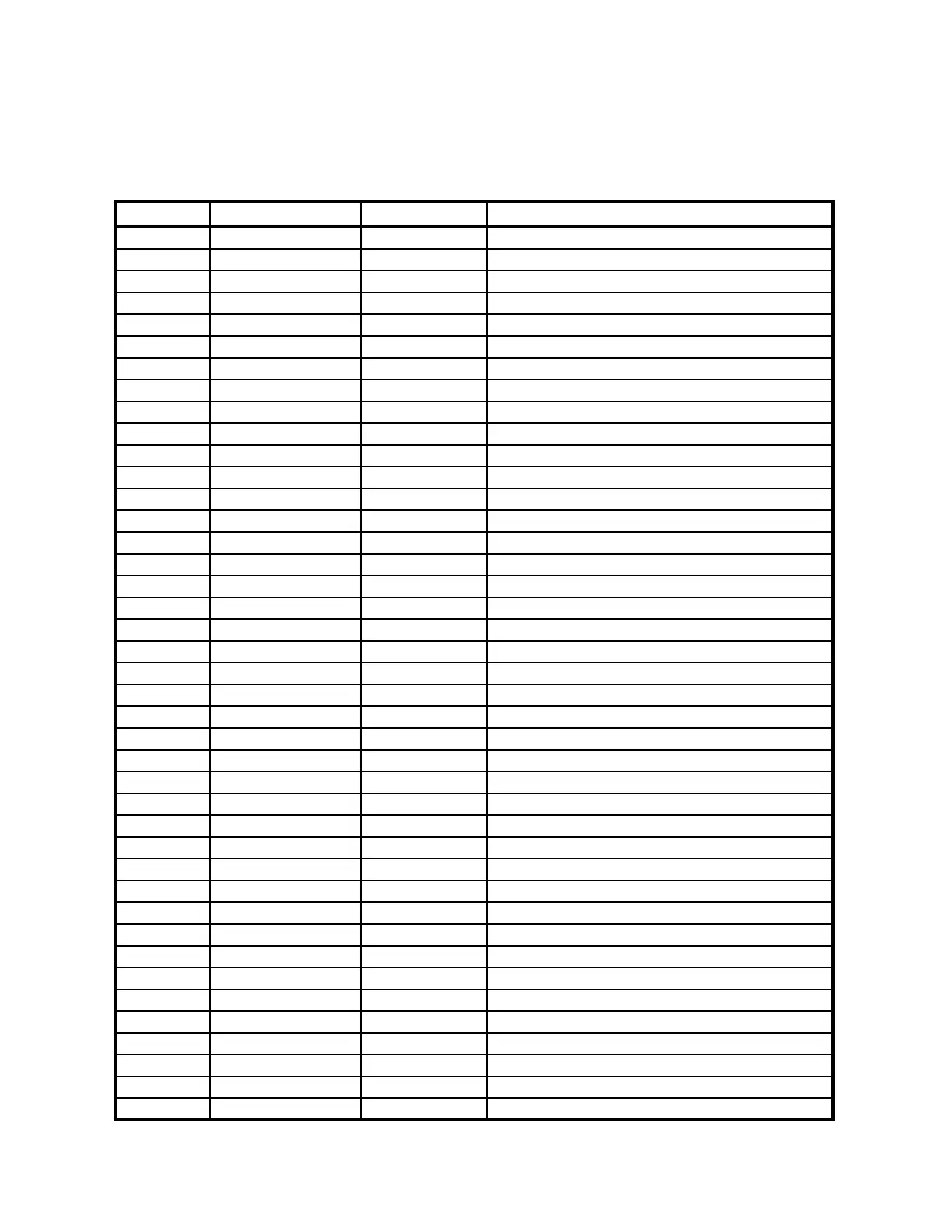
Pin No. Pin Name Input/Output Function
1 ~ 14 KO14 ~ KO1 O Key common signal
15 ~ 22 KI8 ~ KI1 I Key input signal
23 BUFON O Chip select for RAM
24 IT2 I Interrupt input
25 IT0 I Interrupt input
26 ~ 46 AO20 ~ AO0 O Address bus
47 ~ 54 IO0 ~ IO7 I / O Data bus
55 OEBO O Output enable signal for RAM
56 WEBO O Write enable si
nal for RAM
57 ~ 64 CS10BO ~ CS3BO O Chip selectin
si
nals
65 OPT7 O Reset si
nal output
69 ~ 72 OPT3 ~ OPT0 O Chan
eover si
nal
73 PORT7 I Receiving terminal for data communication
74 PORT6 I Receiving terminal for data communication
75 PORT5 O Transmitting terminal for data communication
76 PORT4 O Transmitting terminal for data communication
80 PORT0 I Low battery message for back-up battery (2.6V)
81 VSS I GND
82 PI I 1MHz clock input
83 PO O 1MHz clock output
84 VDD I +3V source
85 XO O 4.3MHz clock output
86 XI I 4.3MHz clock input
87 VCC I +3V source
88 VREG2 O Volta
e for main switch detection
89, 90 TS1, TS2 — Test terminals of factor
purpose onl
91 VSSR I GND
92 BZZ1 O Buzzer si
nal output
93 BZZ2 O Buzzer si
nal output
94 VSS I GND
95 OCLK O Clock output
96 ITOFF I Switchin
terminal from main switch
97 TEMU — Test terminals of factor
purpose onl
98 SW I Receivin
terminal for reset switch
99 VDB I +3V source
100 VREG1 — Test terminals of factor
purpose onl
101 VREG4 O +3V source for ROM
102 VREG5 — Test terminals of factor
purpose onl
103 VDT1I I Forced power off detecting terminal (2.3V)
104 VDT2I I Low battery message for main battery (2.5V)
105 VREG3 — +3V source for RAM
PIN FUNCTION
CPU HCD62121A02 (HC-3017) : COB
NOTE: The CPU is bonding on the PCB. If the CPU is defective, replace the Z888-1 PCB ass'y
because the CPU cannot be replaced.
 Loading...