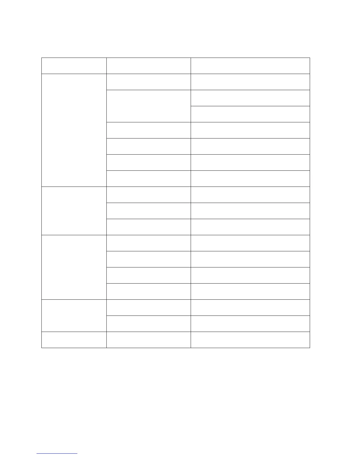
— 11 —
TROUBLESHOOTING
Nature of Trouble Faulty Block Checkpoint
No power Power Jack (J1) Jack contact.
Power IC (IC1: CA5668) Pin 8 should have +5 V.
Pin 6 should provide + 5V when pin 10
receives + 5 V.
Reset IC (IC4: S8053ANO)
Pin 1 should provide a low level pulse when
an AC adapter is connected.
Power Switch
Pin 22 of CPU should receive a trigger
pulse when turning on the switch.
Main Clock Generator (X1) Check oscillation at pin 34 of CPU.
CPU (LSI1: MSM6626-01)
Pin 12 should provide +5 V when turning on
the power switch.
No sound at all Power Amp. (IC2: LA4127) Check output waveforms of pins 9 and 12.
CPU (LSI1: MSM6626-01) Check output waveforms of pins 25 and 26.
ROM (LSI2: MN232000CUQ)
Check CE signal of pin 10, and OE signal
of pin 12.
Distorted sound ROM (LSI2: MN232000CUQ) Check address/data bus.
CPU (LSI1: MSM6626-01) Check output waveforms of pins 25 and 26.
Power Amp. (IC2: LA4127) Check output waveforms of pins 9 and 12.
Power IC (IC1: CA5668)
Check voltages of pins 2 (+9 V) and 6
(+5 V).
All or certain keys do
not function
CPU (LSI1: MSM6626-01)
Check KO signals of pins 1 to 4, and 74 to
80.
Key Matrix Open circuit on KO or KI line.
A certain key does not
function
Key Matrix Dust on the contact.
 Loading...