— 4 —
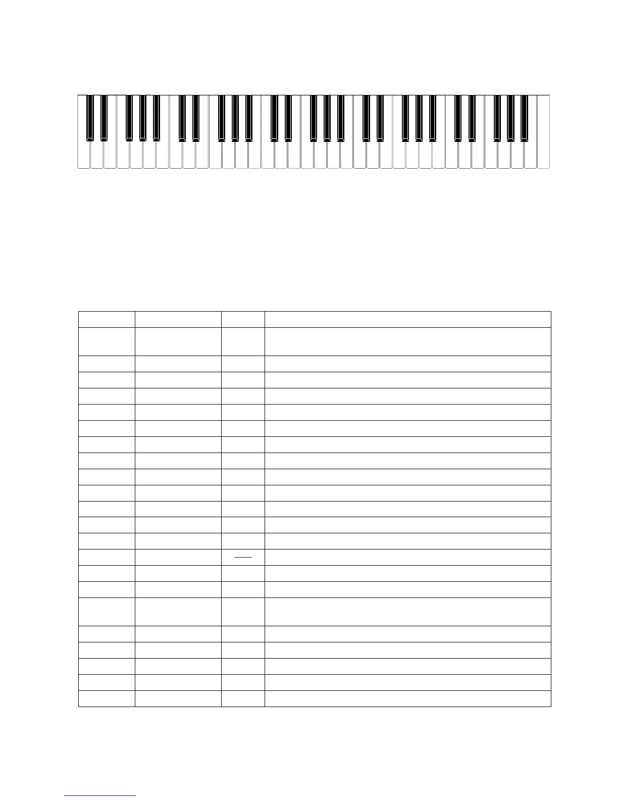
F#3 G#3
A#3 C#4 D#4
F#4 G#4
A#4
C#5
D#5
F#5 G#5
A#5
F3 G3 A3 B3 C4 D4 E4 F4 G4 A4 B4 C5 D5 E5 F5 G5 A5 B5
C6
D#3
C2 D2
E2
F2
G2
A2 B2 C3 D3
E3
B6A6G6F6E6D6
C7
C#3A#2G#2
F#2D#2
C#2
A#6
G#6F#6D#6
C#6
CPU (LSI1: MSM6626-01)
The CPU reads sound data from the ROM in accordance with the pressed key and the selected tone; the
CPU can read rhythm data simultaneously when a rhythm pattern is selected. Then it provides the left
and the right channels' waveforms separately, by converting the data into the waveforms with two built-in
DACs. The CPU also controls keys, switches, and LEDs.
The following table shows the pin functions of LSI1.
Pin No. Terminal In/Out Function
1 ~ 10
74 ~ 80
KO0 ~ KO16 Out
Using time sharing, the terminals provide key and switch
scan signals, and LED drive signals.
11 KO17 Out Clock output for the LED driver
12 KO18 (APO) Out APO (Auto Power Off) signal output.
13 KO20 Out Not used.
14 ~ 21 KI0 ~ KI7 In Input terminals from the keys and switches
22 -MI In Power ON trigger pulse input.
23 -RESET In CPU reset signal input.
24 REFH In Low level reference voltage input for the built-in DAC
25 AVDD In +5 V source for the built-in DAC
26 ROUT Out Right channel sound signal output
27 LOUT Out Left channel sound signal output
28 AGND In Ground (0 V) source for the built-in DAC
29 REFL In High level reference voltage for the built-in DAC
30, 31 TEST1, TEST2 Not used. Connected to ground.
32 GND In Ground (0 V) source
33, 34 COSI, COSO In/Out 43.45 MHz clock input/output
35 VDD In
+5 V DC source. Regardless of the power switch position,
the terminal always receives +5 V DC.
36 -CE Out Chip enable signal output. Low effective.
37 -OE Out Read enable signal output. Low effective.
38 ~ 40 ADR17 ~ ADR19 Out Not used.
41 ~ 57 ADR0 ~ ADR16 Out Address bus for the ROM
58 ~ 73 DIN0 ~ DIN15 In Data bus for the ROM
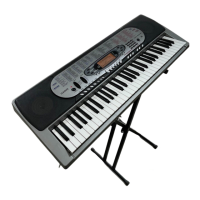
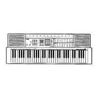
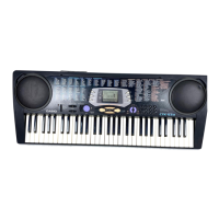
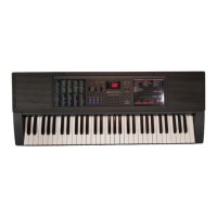
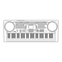
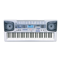
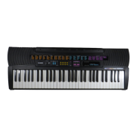
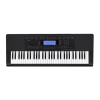
Nomenclature of Keys
 Loading...