— 14 —
(2) Non-port pins (2/2)
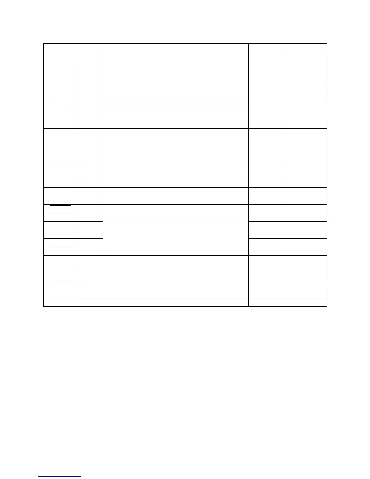
Pin Name
AD0 to AD7
A8 to A15
RD
WR
WAIT
ASTB
ANI0 to ANI7
ANO0, ANO1
AVREF0
AVREF1
AVSS
RESET
X1
X2
XT1
XT2
VDD0
VSS0
VDD1
VSS1
VPP
IC
I/O
I/O
Output
Output
Input
Output
Input
Output
Input
Input
—
Input
Input
—
Input
—
—
—
—
—
—
—
Function
Lower address/data bus when expanding memory
externally
Higher address bus when expanding memory
externally
Strobe signal output for read operation from external
memory
Strobe signal output for write operation to external
memory
Wait insertion when accessing external memory
Strobe output externally latching address information
output to ports 4 and 5 to access external memory
A/D converter analog input
D/A converter analog output
A/D converter reference voltage input (also functions
as analog power supply)
D/A converter reference voltage input
A/D converter, D/A converter ground potential. Use
the same potential as VSS0.
System reset input
Crystal connection for main system clock oscillation
Crystal connection for subsystem clock oscillation
Positive power supply for ports
Ground potential for ports
Positive power supply (except ports and analog
block)
Ground potential (except ports and analog block)
High-voltage application for program write/verify.
Internally connected. Connect directly to VSS0.
After Reset
Input
Input
Input
Input
Input
Input
Input
—
—
—
—
—
—
Input
—
—
—
—
—
—
—
Alternate Function
P40 to P47
P50 to P57
P64
P65
P66
P67
P10 to P17
P130, P131
—
—
—
—
—
—
P07
—
—
—
—
—
—
—
 Loading...