— 11 —
M
1
2
3
4
5
6
7
8
9
10
11
12
13
14
15
16
17
18
19
20
21
22
23
24
25
26
27
2
3
4
5
6
7
8
9
10
11
12
13
14
15
16
17
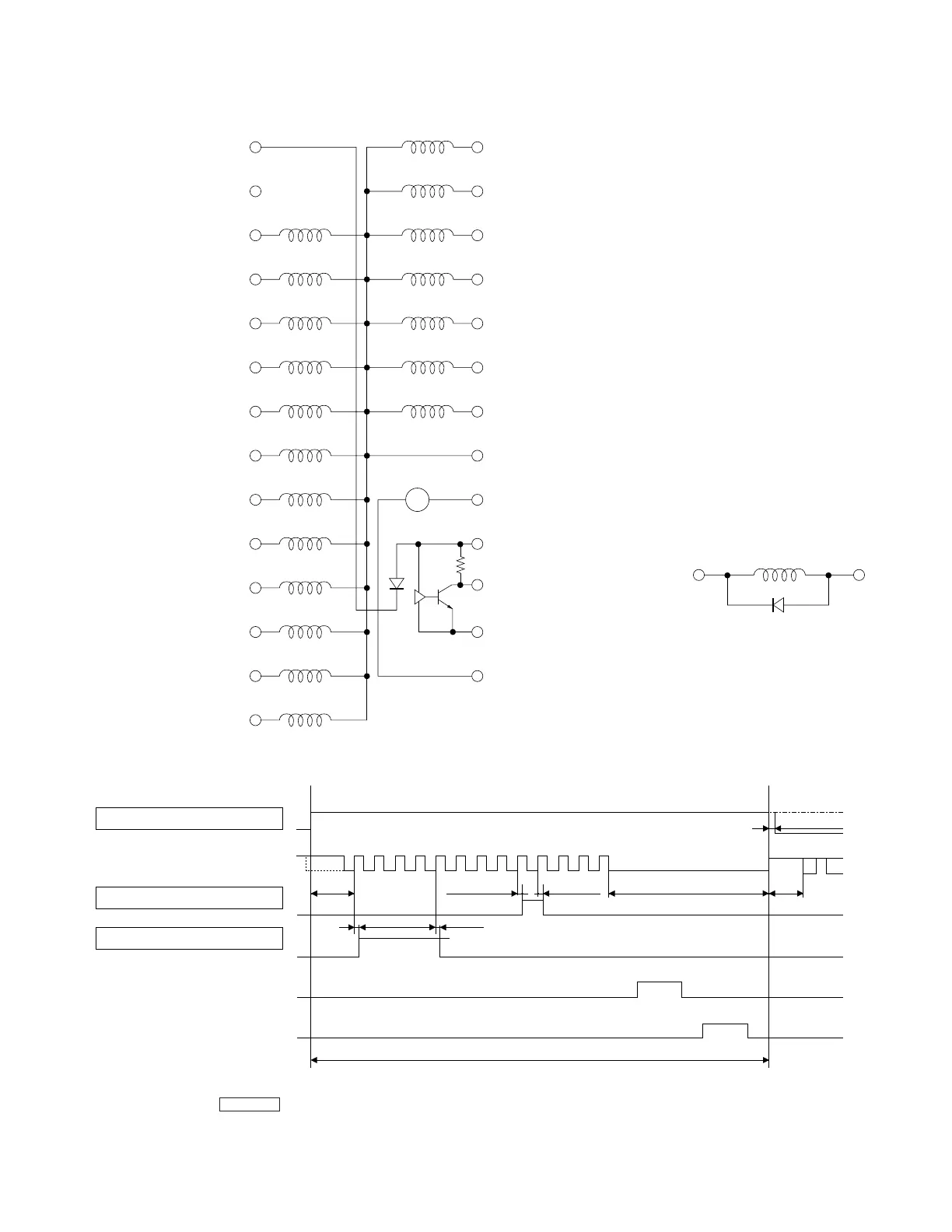
Character selective
magnet column No.1
Ribbon shift magnet
Electromagnet (+)
Motor power
supply (+)
Detector power
supply (+)
Timing signal
Detector power
supply (–)
Motor power
supply (–)
RD terminal
(Not used)
Character selective
magnet column No.1
Electromagnet (+) Driver
(Example of compatible diode:
1S2075K or equivalent)
Connection Pin No. ConnectionPin No.
Motor power ON/OFF
Character selective magnet No.n
Ribbon shift magnet
Timing signal
(Print operation)
(Normal paper feeding operation)
T0 T1 T2 T3 T4 T5 T6 T7 T8 T9 T10 T11 T12
8
0.7ms max.0.7ms max. 80.0ms min.
0.7ms max.0.7ms max.
8.0ms min. 2.0ms min.
TS T(0)
0.2ms max.
Typ. 285.7ms
*2
*1
7-3. Printer Pin Arrangement Diagram
Notes:
1. Column numbers match
the physical arrange-
ment of the columns on
the print wheels.
2. Column numbers are as-
signed from 1 to 18 from
the frame motor side.
3. Pin numbers are as-
signed from 1 to 27 from
the frame motor side.
4. The spark arrestor diode
is connected as shown
below.
Notes:
1. The signals in must be prepared by the user.
2. The pulse is indicated by a dot-dash line (*1) is generated for continuous printing. The next print cycle can start
immediately after the leading edge of the timing signal Ts.
3. As shown by a dashed line (*2), the timing signal may go low at motor power-on or upon reception of a Print command.