— 71 —
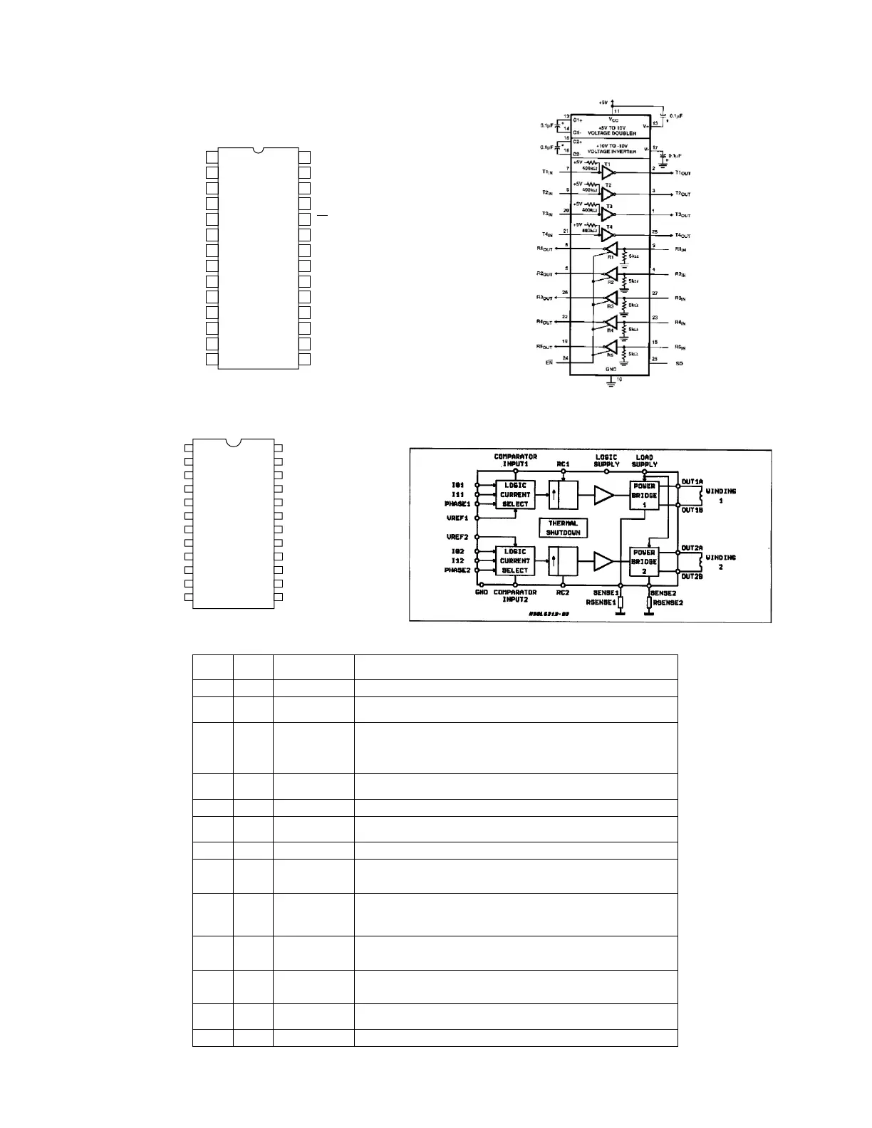
4. L6219DS (IC35, 36)
3. HIN211CA-T (IC1, 2, 3)
1
HIN211E (SOIC, SSOP)
TOP VIEW
2
3
4
5
6
7
8
9
10
11
12
13
14
T3
OUT
T1
OUT
T2
OUT
R2
IN
R2
OUT
T2
IN
T1
IN
R1
OUT
R1
IN
GND
V
CC
C1+
V+
C1–
28
27
26
25
24
23
22
21
20
19
18
17
16
15
T4
OUT
R3
IN
R3
OUT
SD
EN
R4
IN
R4
OUT
T4
IN
T3
IN
R5
OUT
R5
IN
V–
C2–
C2+
Vs (LOAD SUPPLY)
SENSE1
COMP, INPUT1
OUT1B
GND
GND
PHASE1
VREF1
RC1
Vss (LOGIC SUPPLY)
OUT1A
OUT2A
SENSE2
COMP, INPUT2
OUT2B
GND
GND
I02
I12
PHASE2
VREF2
RC2
I01
I11
1
2
3
4
5
6
7
8
9
10
11
12
24
23
22
21
20
19
18
17
16
15
14
13
See pins 5;21.OUTPUT A1;21;2
Connection to Lower Emitters of Output Stage for Insertion of Current Sense
Resistor.
SENSE
RESISTOR
3;234;42
Input connected to the comparators. The voltage across the sense resistor is
feedback to this input throught the low pass filter RC CC. The higher power
transistors are disabled when the sense voltage exceeds the reference voltage of
the selected comparator. When this occurs the current decays for a time set by R
T
C
T
(t
off
= 1.1 R
T
C
T
). See fig.1.
COMPARATOR
INPUT
4;225;41
Output Connection. The output stage is a “H” bridge formed by four transistors and
four diodes sultable for switching applications.
OUTPUT B5;21
8;38
See pins 7;18.GROUND6;19
6;7;17
Ground Connection. With pins 6 and 19 also conducts heat from die to printed
circuit copper.
GROUND7;18
29;39;
40
See INPUT 1 (pins 9;17).INPUT 08;20
16;37
These pins and pins 8;20 (INPUT 0) are logic inputs which select the outputs of the
comparators to set the current level. Current also depends on the sensing resistor
and reference voltage. See Functional Description.
INPUT 19;1719;30
This TTL-compatible logic Inputs sets the direction of current flow through the load.
A high level causes current to flow from OUTPUT A (source) to OUTPUT B (sink).
A schmitt trigger on this input provides good noise immunity and a delay circuit
prevents output stage short circuits during switching.
PHASE10;16
20;27
A voltage applied to this pin sets the reference voltage of the comparators, this
determining the output current (also thus depending on Rs and the two inputs
INPUT 0 and INPUT 1).
REFERENCE
VOLTAGE
11;15
21;26
A parallel RC network connected to this pin sets the OFF time of the higher power
transistors. The pulse generator is a monostable triggered by the output of the
comparators (t
off
= 1.1 R
T
C
T
).
RC12;14
22;25
Supply Voltage Input for Logic Circuitry.V
SS
-LOGIC
SUPPLY
1324
Supply Voltage Input for the Output Stages.V
S
-LOAD SUPPLY2444
PLCC
(*)
PDIP &
SO
Name
PIN FUNCTIONS
Function
BLOCK DIAGRAM
 Loading...